What caused the toasted port on the microcontroller? I’m working always on a electrostatic dissipative mat, so the only possible reason is a conflicting situation on the data bus. I found a sequence in my source code where Port C of the controller and the external SRAM were both set to output. Shit happens!
I modified the circuit so that the output enable pins of the SRAM and the DAC-latch are connected, hence now the SRAM is driving the data bus only during the active periods of a frame. That limits my chances of spoiling the circuit again as there is simply no time to fool around when every cycle counts.
Today I replaced the defective ATmega1284 by a new one, adjusted some fuses, burned the last development version of the firmware aaaand look what we’ve got:
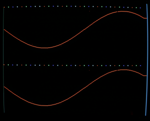
Yeah! Now we are talking! 🙂
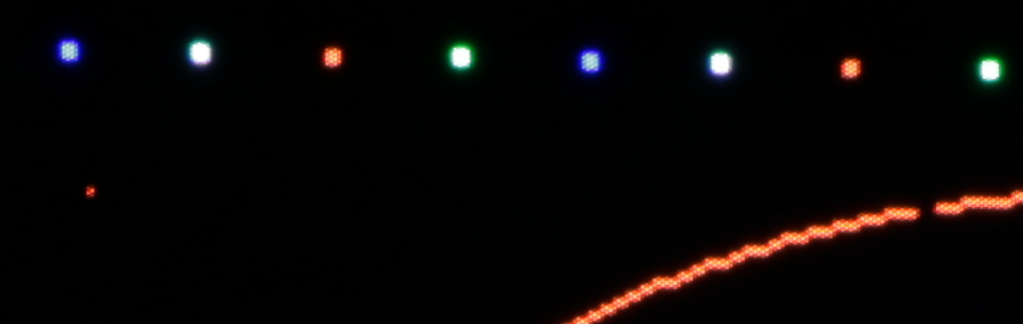
It’s far from being perfect, but it’s doing much better than I expected. Only a few unplanned pixels due to EMI are visible (see below: the small red dot on the left).
There is a discontinuity in the sine wave at x = 256 and if you look closely you’ll notice a slightly greater distance between the red pixel and the green pixel above that gap than between the other pixels. This might be an off-by-one error in the pixel drawing routine or the result of two more clock cycles when switching to the next memory page (256 bytes). The sine wave ends in a flat line, which most likely means the shut-off of the DAC is late. I have currently no clue where the blue-grey vertical lines in the leftmost / rightmost positions come from, though.
I must admit that the desperate hurry during the last few days of RetroChallenge left me with a suboptimal wiring scheme. My decision to use a single port for the low byte and high byte (via a latch) of the address wasn’t particularly favorable. Every pixel has to be drawn within two clock cycles. That works fine until the address counter of a line reaches 255. Now we need to increment the high byte of the address and set the low byte to zero:
– increment address high byte register (1 cycle)
– set transparent mode (1 cycle)
– output address high byte register (1 cycle)
– set latched mode (1 cycle)
– clear address low byte register (1 cycle)
– output address low byte register (1 cycle)
Obviously that does not fit. Here is my workaround:
– set address pin A16 to high (2 cycles)
It works, but the resulting memory scheme is weird:
0, 1, 2, 3, … 255, 65791, 65536, 65537, 65538, … 65598
Ok, it’s not as bad as it looks like at first glance. Every memory scheme is just a human conception/idea. The memory chip doesn’t care about the address sequence at all. As long as we use the same address when reading or writing a specific byte everything is honky-dory. However, we waste 192 bytes per line this way. Version 2.0 of CHRE will take care of this issue…
In fact, the gap we’ve seen in the sine wave was caused by an off-by-one bug and wasted cycles. And the DAC-latch timing was wrong. Both issues could be fixed easily. In addition the vertical resolution has been reduced from 480 to 240.
So, now we have 320 by 240 at 256 colors! That was one of my goals for RetroChallenge. Accomplished. But way too late. 🙁
Anyway, playing with this graphics board is fun:
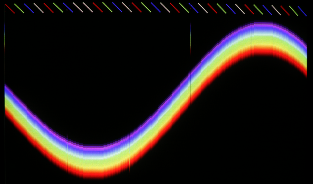
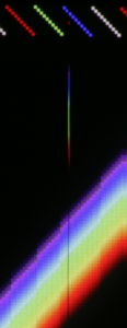
Unfortunately we see some spooky vertical lines now…
 To be continued…