RC 2017/04 – Alternative Schematics

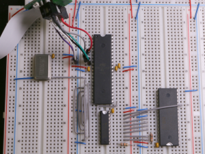
Time is short so let’s skip the part where we draw schematics. I thought it would be more fun to show you how the circuit develops and explain it along the way.

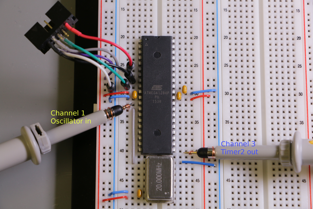
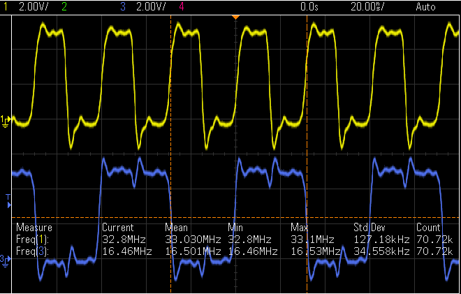
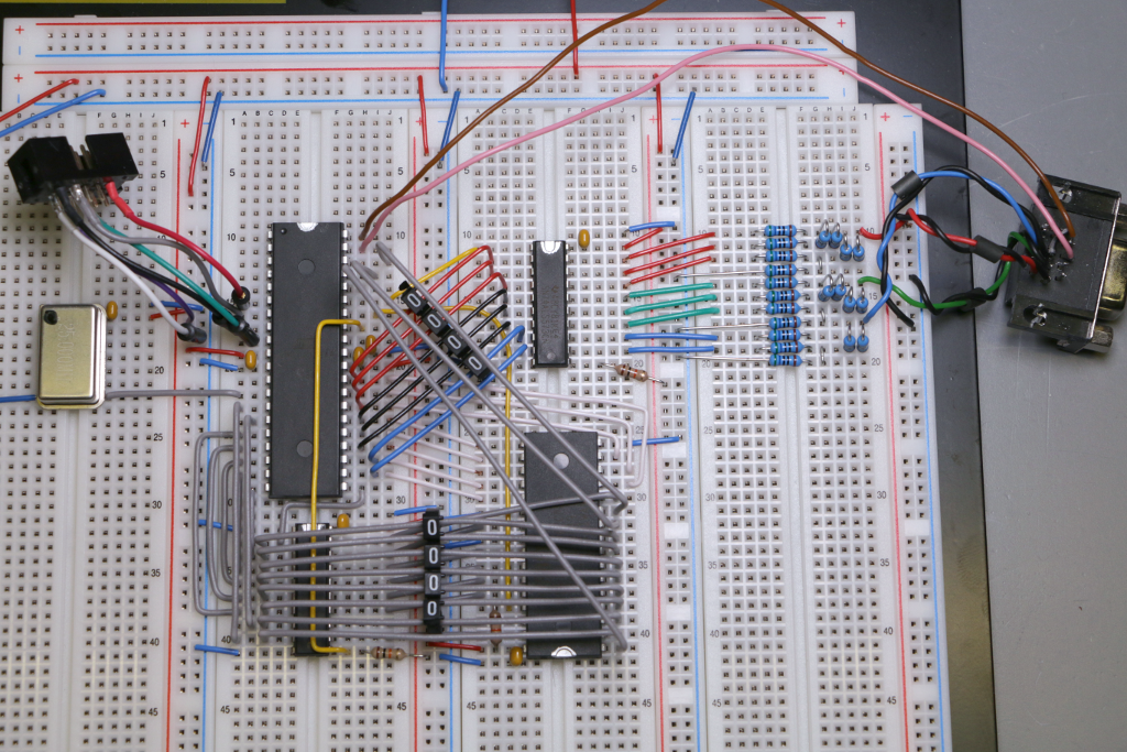
A golden rule in (high speed) digital circuit layout is to keep wires/traces as short as possible and to increase the spacing between adjacent wires/traces. That helps to reduce electromagnetic interference, e.g. cross talk. Therefore the previously used test circuit has been rearranged to get the oscillator out of the way. The grey wire between the silvery can on the left and the biggest chip on the board is our clock line feeding a square wave of 25 Mhz @ 5 Vpp into the ATmega1284.

Blue wires are  signal ground,
red wires are  supply voltage,
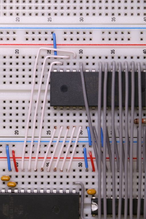
grey wires are  address lines and clock lines,
white wires are data lines ,
yellow wires are control lines,
(SCNR, read: ‘data lines’ and ‘control lines’)
beige drops are  decoupling caps,
beige or blue cylinders with colored stripes are  pull-up resistors,
unless otherwise noted.

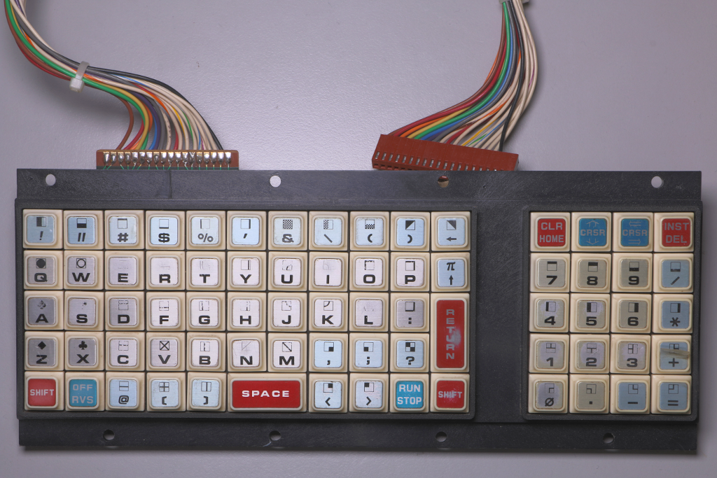
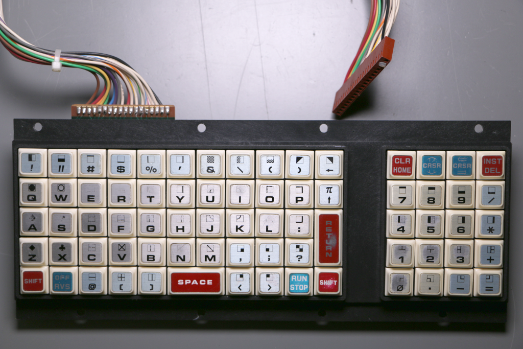
First exception: A bunch of colorful wires is leading to a connector and a flat flex cable at the top left. These are used to program the microcontroller (MCU).

There’s an address latch (74ALS573) below the MCU. Yes, I know. The ALS type is too fast for the task and may cause additional EMI issues. Unfortunately I don’t have (or can’t find) the HC type. Living countryside doesn’t help when trying to buy electronic parts on a weekend either.

The external SRAM (BS62LV4006) is situated on the right. Nineteen address lines are required to access the full 512KB. Add eight data lines, eight lines for communication to the user port of  the PET 2001, three control lines, two video sync lines and you’ll get  ERROR! OUT OF I/O PINS!  The solution is a buffer store aka latch:

Port D of the ATmega is connected to the SRAM via the address latch. Thus it can output the first byte of an 19-bit-address while in transparent mode, then switch to latch mode. The address latch keeps this bit pattern on its output pins, regardless of any state changes on its inputs until it is switched back to transparent mode. Now Port D can output the second address byte.

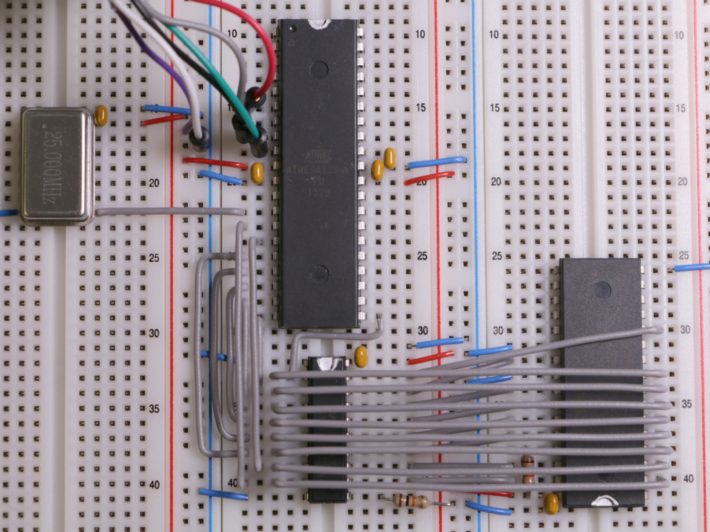
Additional eight wires are routed from Port D to address pins on the other side of the SRAM.

Avoiding long wires means implementing a second layer. This is a small, easy project on a breadboard.

Now we connect Port C to the data bus…

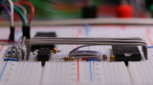
… and add a simple R-2R resistor ladder network as Digital Analog Converter (DAC):


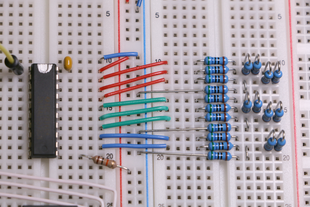
Please note that there is a second latch! It will separate the data bus from the DAC while data is written to the SRAM, because otherwise we would get flicker at least. Most likely the horizontal and/or vertical synchronisation would fail.

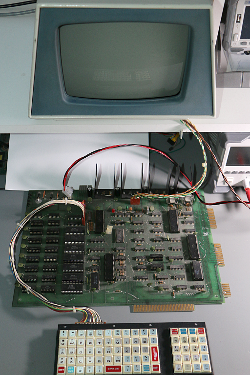
The last picture shows the complete CHRE circuit including a third layer of address lines, five control lines (latches, SRAM Read/Write, Hsync, Vsync) connected to Port A and some spacers on the second layer.

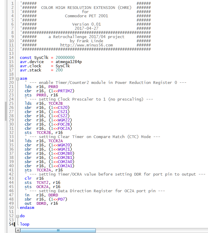
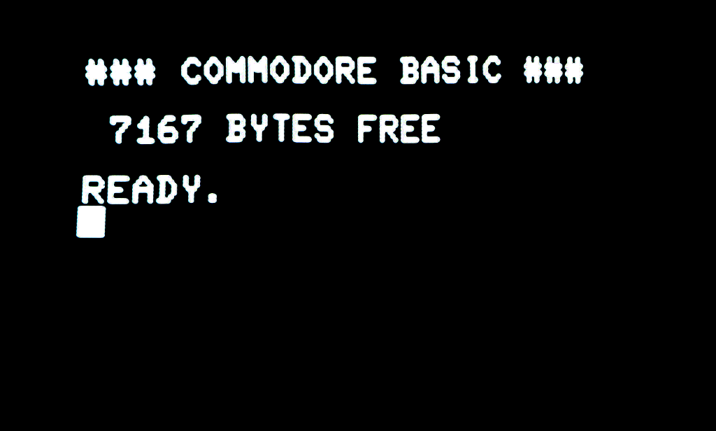
Now on to firmware development. Hurry up!!! Only 1.5 days to go…

RC 2017/04 – Breadboard Time

It’s a matter of common knowledge that a breadboard isn’t suitable for high frequency circuits. But 0.025175 GHz is almost DC, right? Not at all! In particular, one will find fast edges, even in most digital circuits that are clocked really slow. It’s not only the system clock we have to worry about when prototyping on a breadboard. These fast edges may contain high frequency components up to several hundred MHz.

Nevertheless I’ll start on a breadboard. Why? To test a few things before going any further. Okay, maybe there is also a tiny bit of curiosity involved. 😉

But before we go to the breadboard we need to do some math. Please stay with me! It’s basic arithmetics only. Promise!

The PET displays 40 x 25 characters using an 8 x 8 pixel monospaced font. The corresponding screen resolution is
40 * 8 = 320 pixels horizontal,
25 * 8 = 200 pixels vertical.
Having this resolution for color graphics would be great, as we could print text in the original PET font side by side to color graphis at the exact same pixel size.

As mentioned before a horizontal resolution of 640 pixels equals to a Dot Clock of about 25 MHz in the VGA universe. For a resolution of 320 pixels the Dot Clock is halved, too (25 Mhz / 2 = 12.5 MHz). The plan is to store the color of a pixel in a single byte, so 2 * 2 * 2 * 2 * 2 * 2 * 2 * 2 = 256 colors are possible (Sorry, but I had to keep a promise. For really advanced mathematicians out there that is 2^8).  Thus the circuit will have to spit out a byte per pixel – that is 12.5 megabytes per second!

All video data resides in external RAM. Transfering a byte (pixel) from external RAM to the DAC (Digital Analog Converter that converts pixel data into VGA compatible voltages) requires four steps:

Precondition: RAM is in read mode

1) calculate RAM address
2) feed address to RAM
3) read color byte from RAM
4) send color byte to DAC

Assuming that each of these steps takes a single clock cycle, a system clock of 4 * 12.5 MHz = 50 MHz is needed. The ATmega1284 is rated for a maximum clock frequency of 20 MHz. Oops.

Fortunately two of these steps are unnecessary. We can avoid steps 3 and 4 by connecting the external RAM data bus straight to the DAC. The microcontroller will act merely as a counter then. Wouldn’t it be easier and cheaper to perform this task with a standard resettable counter chip? Well, it’s possible for sure (PET 2001 video circuit consists of 74xxx logic only), but in my view it’s more convenient and flexible to substitute a microcontroller for a bunch of logic chips here. Anyway, in both cases we end up with dealing with two logical steps. The question is if the above assumption is true: How many clock cycles does the ATmega really take to perform these steps? Ooookay, the party is over! We’re talking assembler and count cycles from now on…

Come on! Stop crying! Real programmers do talk assembler and do count clock cycles. End of story.

The ATmega1284 datasheet (in fact it’s more of a databook), chapter 29, Instruction Set Summary, is our friend: It takes one cycle to increment or decrement a register and it takes one cycle to output a register value to an I/O port. Therefore a pixel can be addressed in two clock cycles. That’s great news! Assumption verified! We need a system clock of only 2 * 12.5 MHz = 25 MHz. …
Only? That’s still 5 MHz more than the 20 MHz the ATmega is specified for.

Guess what? First task on the breadboard will be pushing the ATmega1284 to its speed limits. I’ve done overclocking on other AVR chips before. A stable external oscillator is key to maximum speed. The test circuit is pretty simple:

Just the controller, an external crystal oscillator, a bunch of capacitors, a programming header and two oscilloscope probes. All tests will be done at 5 volts. We start at 20 MHz to make sure everything is working correctly when the clock is within specification.

The program is quite simple as well. It’s the setup of Timer2 to toggle PD7 on compare match and an endless loop doing nothing:

According to the datasheet this configuration is specified for a maximum toggle frequency of SysClk / 2. A quick look at the scope verifies that the frequency at PD7 is about 10 MHz. So far so good.

Now we’ll raise the frequency until the circuit stops working correctly. My junk box offers 25, 28.322, 32, 33, 36, 40, 48 and 50 MHz…

Tataaa!!! Aaand the winner is:

33 MHz!!!

Wow! That will give us a reasonable safety margin when running at 25 MHz!

Only three days left and counting…

RC 2017/04 – Real Deal

Although I enjoyed to see the PET 2001 being safe and sound again, it was no big deal as most of the work had been done before this RC. The real challenge will be to build a color high resolution graphics extension board for the Commodore PET 2001 and some later models of the PET/CBM series. I’ll name that board ‘CHRE’ for ‘Color High Resolution Extension’ to illustrate it’s affinity to my RC 2015/7 project (HRE) which was monochrome only.

In contrast to the Commodore C64 the PET/CBM 2000, 3000, 4000 and 8000 models were not equipped with pixel graphics or color at all. Therefore we cannot enhance any internal system, we’ll have to start from scratch. What kind of screen should we use? TV-set? 4k curved OLED? The latter isn’t really a retro thingy, so no. A telly would fit to the 40 characters per line of a PET 2000, 3000 and 4000 model but I’d like to support an 80 column text mode (monochrome) for the 8000 models some day. While it’s possible to display 80 columns on a TV-set, the readability won’t be great. Thus we’ll cancel the telly and stick with a more modern standard called VGA. VGA monitors are still available at stores and The Bay. You may find a VGA input connector even on some present-day display systems.

VGA supports multiple resolutions and color modes. There are two limiting factors when it comes to graphic modes:
1) Dot Clock (frequency with which pixels are illuminated on the screen)
2) Video RAM (memory where pixel data is stored).

For a very common VGA mode of 640 by 480 pixels by 256 colors we would have to deal with a Dot Clock of 25.175 MHz and would need 307200 bytes of Video RAM (for you youngsters out there: that is 0.025175 GHz and 0.0003072 GB). Our PET/CBM CPU is an 8 bit processor running at about 1 MHz. Its max. address space is 64 KB. Even 160 by 120 pixels would require a Dot Clock of more than 1 MHz. Magic aside, how can we support any useful VGA mode? Well, we’ll need some kind of GPU and external RAM.

I’ve choosen the Atmel megaAVR series of 8 bit microcontrollers for the GPU. The biggest (in terms of I/O pins and features) and fastest (in terms of instructions per second) controller of this series is the ATmega1284. That’s not exactly true as its little brother ATmega644 needs a cycle less at jump instructions. It remains to be seen if these few cycles are relevant when calculating any time-critical parts of the firmware (aka cycle counting). The external VRAM will be a BSI BS62LV4006PCP55. That’s a 512K x 8 bit 55ns CMOS SRAM in a PDIP-32 package. The first homecomputers with color graphics used weird memory layouts to cope with memory and speed constraints. Our blisteringly fast GPU and nearly infinite VRAM will hopefully allow for a nice memory layout…

So the plan is to head for the following goals:

– color graphics mode with 160 x 200 pixel resolution at 16 colors or better
– color text mode with 40 x 25 characters at 16 colors or better
– minimally invasive connection to the PET 2001
– implement simple graphic functions in GPU firmware
– implement PET control software as a BASIC extension

Only 8 days left. Oops!

RC 2017/04 – PET Testing

With a reassembled keyboard, a previously repaired CRT and a previously repaired mainboard we’re ready to stick the PET together and fire it up for further testing. We use separte channels on the power supply for mainboard and CRT and turn Over Current Protection on – just in case…

A piece of white paper behind the mainboard will help to localize any magic smoke trying to escape. No, hopefully not! It’s  just to hide the usual random stuff scattered on a bench.

Well, then! Take a deep breath! Cross your fingers! Push power button #1 (CRT)! Oookaaaay. No arcing. No smoke. OVP did not trip. A current flow of about 130 mA sounds reasonable. So far, so good. Take another deep breath and turn on channel #2 (mainboard)!

Uuaaah!!! I’d like to point out that this is not exactly what I was looking for. But no arcing, no smoke, no OVP trip either. About 2.5 A current flow is ok as well.

To the oscilloscope!

Horizontal sync, vertical sync and pixelstream are looking good, so we can’t blame it on the main circuitry. Oh, great! That means we’ll have to do probing on the CRT circuit board – close to the high voltage area. Any volunteers?

Fortunately it was much easier than I thought. Most errors are sitting in front of the machine, as the saying goes. You bet! I knew that the CRT needed 12 V to operate and that was precise what the power supply was set to. Nothing to complain, right? Well, as soon as I looked at the schematic I realized that the 12 V voltage regulator is situated inside the CRT and not on the mainboard. It’s a standard 7812 type regulator, so we have to add the dropout voltage of 2 V to the regulated output voltage. After changing channel #1 to 14.5 V the PET welcomes the RetroChallenge audience:

YEAH! That feels good! 🙂 A trivial BASIC program works as intended:

It’s running at cyberspeed <ahem>, so the last digit shows some ghost pixels. I checked the tape interfaces with an external Datassette and both were fine. But all attempts to get a device running on the IEEE-488 bus (aka GPIB) failed. Before we investigate this issue any further, we need to perform some more comprehensive tests:

Ahhh, it’s been the golden age when humans were able to outplay computers…

Ok, RetroChallenge is no amusement hall. We have a mission! Let’s track the IEEE-488 issue down! There are two 6520 Peripheral Interface Adapters (PIA) in a PET 2001, one acts as IEEE-488 bus controller, the other one mainly as keyboard controller and as datassette port controller to some extend. Keyboard and datassette ports have been verified. A simple swap should tell if the GPIB PIA is dead. When I had lifted the GPIB PIA out of its socket I found some residue on the pins as well as on the socket.

A toothbrush in collaboration with denatured alcohol removed it easily. A quick check (after PIA had been reinserted) verifies we have a working GPIB now! Hurray!


I call that a running system – the PET has been reanimated.  RetroChallenge Mission #1 accomplished.

RC 2017/04 – Keyboard Puzzle

Ok, let’s get started! As the disassembled PET takes a lot of space on the bench, it will be my first goal to put all parts back into the chassis. Most of the issues this computer had when I got it, should have been fixed during the previous repair sessions (which are not part of this RC entry), but it’s more convenient to perform measurements and/or soldering while the mainboard lies on the bench. So testing will go along with the reassembling procedure, just in case something has been overlooked.

Talking to computer systems of the 70s wasn’t like talking to a modern smartphone – we were forced to use a special device named ‘keyboard’ that looked similar to this one:


As you can certainly imagine, it’s been hard work to use such a keyboard, so blood, sweat and tears build up on the device after a while. In this case ‘a while’ translates to ’40 years’ and I was surprised to find only minor deposit on the keycaps…


… but decided to get rid of it anyway. Tissue, denatured alcohol, time and some more sweat got me to the point where the surface started to shine again:


Unfortunately the alcohol partially dissolved the labelling, so I used it only for cleaning the plastics. And to be honest, the whole process was agonizingly boring! It will take a looooong time to choose a suitable detergent for cleaning the top of the keycaps…

During the cleaning it crossed my mind that arranging things diffently might improve the usability of the keyboard.

I really enjoyed this puzzle although I heard a ghostly voice all the time shouting ‘Give me a Q! Give me a W! Give me an E!’ and so on. Can’t remember exactly where I heard this voice in my youth. Sesame Street? Most likely. Everything went well, except the ‘Q’-key. The keycap did not fit and guess what happened? Statler and Waldorf were laughing at me ‘When a spring sprang in spring! <chrrrrhrrhrr><chrrrr>’.

Glueing the keycap to this other light grey thingy wasn’t an option, but a few layers of flimsy PTFE tape made my day.

I’d like to believe that one can tell the difference…