A quite time consuming task at top priority (aka life) stopped me from working on this project. In the meantime Retrochallenge 2016/01 is open to entrants and guess what my entry is!
Category: RC 2015/7
RC 2015/7 – Follow up #1
A month has past since the end of Retrochallenge 2015/07 and … I miss the feeling! Yep, I miss the Retrochallenge feeling. That is, working on a challenging project just for fun. Specifically working on interesting stuff for ancient computers. Ok, I assume you’re one of the 0.0236986301 ppm of world population who do understand what I’m talking about if you’re reading this at all.
Therefore I won’t wait for RC 2016/01. I’ll continue to work on my RC 2015/07 project and turn the proof of concept into a working prototype. To be honest I already restarted the project and didn’t tell you. 😉
Finding the Vsync bug that showed up in the demo video (RC 2015/7 final post) has been the first task. As I have mentioned before it is critical to count every single cycle within the video output routines. And what happens when you work after work ’til late night? You sometimes can’t count anymore! The error was caused by a not equally timed program path. There is a reason why they call an oscilloscope “electronic engineer’s best friend”. Would have been clever to verify the counted cycles with my friend somewhat earlier…
Optimizing the code gave me some additional free cycles so I could increase the resolution from 640 by 250 to 648 by 256. It’s nothing to write home about but the extended resolution allows to draw small symbols outside the CBM text region which might come in handy in certain cases.
One page consumes 648 * 256 / 8 = 20,736 bytes of external SRAM. The size of the installed SRAM is 131,072 bytes (128k * 8 bit). How do we make use of the remaining memory? Several framebuffers! The ATmega162 can address 64k of external SRAM minus 1k internal SRAM minus 256 bytes registers. These 64,256 bytes contain 3 framebuffers and leave 2k for future ideas. The other half of the SRAM chip can be reached by banking. That equals to six independend framebuffers and two 2k free memory blocks in total.
The framebuffers can be used in two modes. In mode 0 all six buffers are orthogonal. In mode 1 only the three buffers in bank 0 are available for drawing while the three buffers in bank 1 are used to implement a second ‘color’. You may call this lower level of brightness ‘dark green’ as well as ‘transparent green’. The following image shows the extended resolution by a border drawn outside the CBM display real estate and explains the meaning of ‘dark/transparent green’.
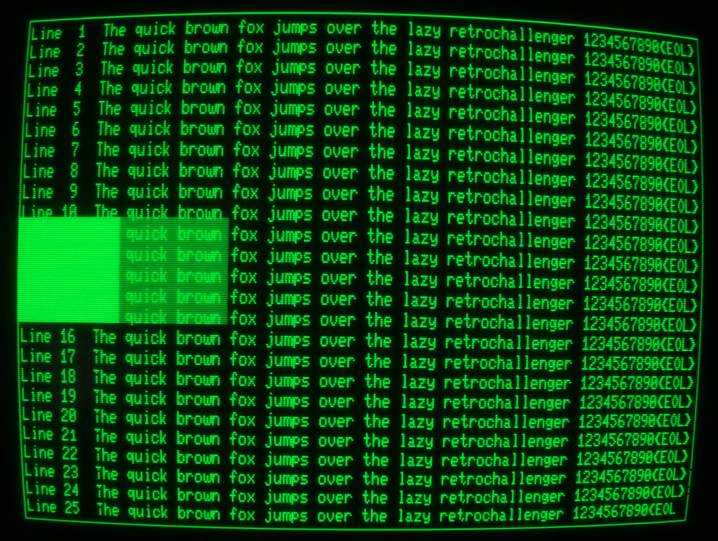 Please take a closer look at the characters ‘T’ in the bottom half of the screen and ‘1’ in ‘Line 21’ as well as the disruption of the right border line. These seem to be side effects of the wild wiring – sometimes present, sometimes absent. EDIT: No, it’s a problem of the CBM mainboard that persists even if I disconnect the HRE completely. Talking about the characters only. The line disruption is most likely a problem of the HRE. And no, it’s not the dust on my camera.
To get the second ‘color’ two associated framebuffers at the same address on different memory banks are used. The video output routine switches between these two buffers at a frequency of 25 Hz. If a pixel at a specific location is set in both framebuffers it will be displayed at full brightness. If it is set in one framebuffer only it will be displayed at half brightness. Due to the fact that CBM text is always displayed at full brightness it will shine through in areas of ‘dark green’.
Unfortunately the applicability of this second ‘color’ is very limited: A refresh rate of 25 Hz implies severe flickering. Adjusting the potentiometer at the back of the screen to reduce overall brightness might help a bit but won’t provide a good display quality.
I plan to modify the user port communication but haven’t come up with a better solution. A first attempt to implement a more sophisticated protocol killed the balanced timing.
RC 2015/7 – Final Post
Ok, Murphy did bug me – as always. I eventually finished a short crapy video that is currently uploading to my Youtube channel. It’s my first video ever and I have no idea if it will be of acceptable quality, but I’m sure you will enjoy my stuttering:
High Resolution Extension demo video
All aims of this RC project have been accomplished. 🙂 I’m astonished that the wild wiring hasn’t caused any severe problems. Yes, there is some jitter and maybe it’s a result of not having a proper PCB – maybe. And there is a loose contact. That’s it. Not half bad!
And the firmware? Well, as you can see in the video there is an issue with synchronisation when line mode is used. Unfortunately I failed to debug it this day. Drawing procedures that have a “longer” execution time will trigger the error. That’s confusing because both sync routines have been implemented as interrupt service routines (ISR). Some investigation is required here…
Ideas for future development? Yes, sure! Character generator, page switching, sprites, DrawRectangle, DrawCircle, …
Retrochallenge 2015/07 has been great fun! Thanks for having me! Looking forward to RC2016/01! 🙂
RC 2015/7 – Home Straight
Engineer’s Log, Labdate 0730.12. We finally reached Warp 5.0! Too bad this starship has been shut down long since.
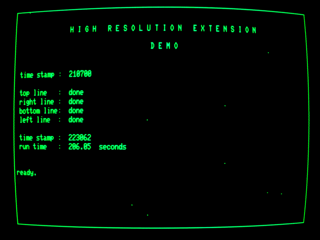
Yesterday I met target #6 of my Retrochallenge project: A very basic Graphical Processing Unit has been implemented. Besides its primary tasks (framebuffer handling, host communication, set pixel at x/y position) the microcontroller features a DrawLine command now. This results in a tremendous speedup:
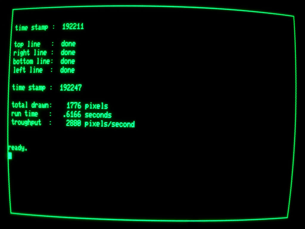
We went from 159 seconds (see previous post) to 0.62 seconds! Instead of sending 1776 single SetPixel commands to the HRE we’re now sending only 4 DrawLine commands. This way we overcome the poor BASIC performance.
The acceleration would be even more impressive if we would compare diagonal lines because in that case we’d have to do some additional calculation in BASIC. I implemented a complete Bresenham line drawing algorithm in the HRE firmware so diagonal lines are supported.
The microcontroller has still plenty of flash memory left for future expansion (about 79%). But I have attained all goals for this Retrochallenge and prefer to spend more time in bed in the upcoming nights. 😉
I’m going to write a demo and to shoot a video in the remaining hours until RC2015/07 ends – provided that Murphy won’t bug me.
RC 2015/7 – Dances With Pixels #3
Engineer’s Log, Labdate 0728.20. Warp 4.8! We’re getting close.
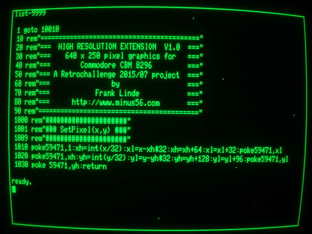
After a close fight against Murphy I finally won the day: The Commodore CBM 8296 is talking to the HRE via the userport. This small BASIC program demonstrates how the communication is handled on the CBM side. It draws a border around the screen in this order:
(x, y) 0, 0 –> 639, 0 –> 639, 249 –> 0, 249 –> 0, 0
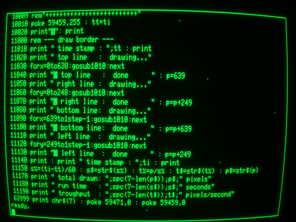
Parts of the program have been squeezed by some methods we used in the early 80th to reduce execution time. These tricks reduced not only the readability of the program but also the runtime from 206 seconds …
… to 159 seconds …

which is still very slow.
If my cell phone cam is able to shoot a video of the program output there will be a final comparison of this pixel by pixel output and the accelerated line output I plan to implement tomorrow.
RC 2015/7 – Dances With Pixels #2
Engineer’s Log, Labdate 0726.15. We are traveling at warp 4.5 now. Scott and Spock are still trying to reach warp 5.
Found the missing pixels. They have been buried under some missing NOP instructions. Hmm, ok, it’s nearly impossible to bury anything under something that is missing but I managed it somehow. 😉
Now HRE has full resolution of 640 x 250 = 160,000 pixels!
A simple interface should read commands from the CBM userport. How do we implement this feature? It depends on the time between successive commands and on the transmission time for a single command. I’ll write a small transmit loop in BASIC and measure the execution time. A datassette has the honorable duty of being responsible for a save and reliable storage.
I don’t care about command structure at this stage. All I want to measure is the time for the fastest possible change of signal levels at the userport (BASIC only). Will the execution speed change if we put two BASIC statements in a single line?
1000 POKE 59459,255
1010 POKE 59471,255:POKE 59471,0
1020 POKE 59471,255
1030 POKE 59471,0
1040 GOTO 1010
 Wow! 7.281 milliseconds! What a blazing speed! That equates to a bandwidth of more than 137.343 bytes/s! Eat your heart out Nvidia!
Putting two statements in a single line doesn’t make any difference.
Ok, let’s assume the 6502 is going to train for CPU olympics. Hence, further calculation will be based on a value of 5 ms to be on the safe side. If we sample the userport at each HSYNC interrupt we get more than 80 samples per level change. That’s more than adequate. Currently there are about 170 free cycles at the beginning of the HSYNC ISR so I intend to handle the userport communication there. It’ll be somewhat challenging because the HSNC ISR must be cycle exact. So what? May I remind you that this is a retroCHALLENGE entry?
Now we should think the protocol through. The absolute minimum number of bytes per command (without considering compression) will be four:
1 byte for instruction (e.g. 1 = SetPixel, 2 = MoveCursor, 3 = DrawLine, …)
2 bytes for X coordinate
1 byte for Y coordinate
Unfortunately the HRE wouldn’t be able to identify the single bytes. For example the command SetPixel(256,1) will translate to $01 $01 $01 $01. Not a single bit does change during the whole data transfer! How do we separate the bytes?
We’ll use only 5 bits of a byte for data and 3 bits for synchronisation. That adds some complexity to the protocol which reduces bandwith even more but we can strive for speed in an upcoming Retrochallenge. 😉
The following table of the three most significant bits shows the unique coding of each byte:
000 => command
001 => X-coordinate low
010 => X-coordinate high
011 => Y-coordinate low
100 => Y-ccordinate high
101 => future expansion
110 => future expansion
111 => future expansion
So we have to transmit a total of five bytes per command.
Looking forward to my first non trivial BASIC program since the 80th. 🙂
RC 2015/7 – Dances with Pixels #1
Engineer’s Log, Labdate 0725.22. Science Officer Spock finally managed to persuade the computer to accept the modification. We are traveling at warp 4.4 now. Warp 5 should be possible, though.
Ok, I swapped pins PE0 and PD0 to free an interrupt for VSYNC detection and added the interrupt service routine. Luckily vertical synchronisation worked right from the start. 🙂
Sadly, tracking down the jitter problem isn’t that easy. At first glance it appeared to be a small difference in frequencies (main clock CBM vs. main clock HRE) so I tried to run the HRE on the CBM’s main clock and it improved somewhat. The jitter disappeared for one or two minutes to be precise – then returned. Cooling spray helped to locate the source of the problem: It’s the hex inverter chip (UD3) that forms the oscillator circuit. Really? I carefully examined the CBM text on the screen and there wasn’t any jitter at all. Only the HRE output showed jitter. Then I touched UD3 with my fingers and the jitter changed or disappeared. Unfortunately I have no spare finger to add to the circuit…
My provisional conclusion: The jitter is caused by the marvellous wiring and perfect grounding/shielding of the HRE board <ahem>. As we are pinched for time I won’t design a proper PCB to solve this problem. Rearranging the cabling helps a bit…
A screen full of equally spaced vertical lines is of avail when checking horizontal sync but otherwise quite boring. A screen full of freaking awesome vertical lines would require variable spacing! Easy! Just change the bit pattern and … fail.
For the first test I wrote a bit pattern to the external SRAM and imported the data in the next cycle to the shift register then clocked the bits out of the shift register to the monitor.
LDI r25, 0b01111110 // load register 25 with bit pattern
ST $8000, r25 // store register 25 value into SRAM
OUT CtrlPort, r19 // load data into shift register
OUT CtrlPort, r20 // start clocking bits out of shift register
NOP // waste one cycle
NOP // waste one cycle
These six instructions take 8 cycles which is the time that is needed to clock 8 bits (pixel) out of the shift register. In other words 8 pixels are loaded and sent out to the monitor in 8 cycles thus allowing for a pixel frequency of 16 MHz.
Along with changing bit patterns for variable line spacing I coded a complete framebuffer handling as it will be needed for a graphic extension. Now I was reading the bit patterns from SRAM and then transferring them to the shift register. It turns out that the byte that has just been read from SRAM stays valid on the data bus for only one clock cycle (when /RD is LOW). The following OUT instruction cannot see this data anymore thus the transferred byte is not correct.
First idea was to send the data (that has been read into a microcontroller register) out to another port and import into shift register from that port. That would work if we had a free port.
Second idea was to handle the external SRAM manually but that would take much more clock cycles and reduce the horizontal resolution.
Third time is a charm: Enable XMEM, read bit pattern from external SRAM, disable XMEM, enable manual output on port A, send bit pattern to port A, import into shift register, start shifting. That results in 9 clock cycles which is still one cycle too many <Ҥ$+#%&/()!!!!> Fortunately the XMEM interface overrides any conflicting port definition if enabled and restores the old definition if disabled. So I could remove the port definition from the framebuffer read sequence and saved a cycle.
Meanwhile I wasn’t positive about vertical lines at all and programmed a bunch of sinewaves instead: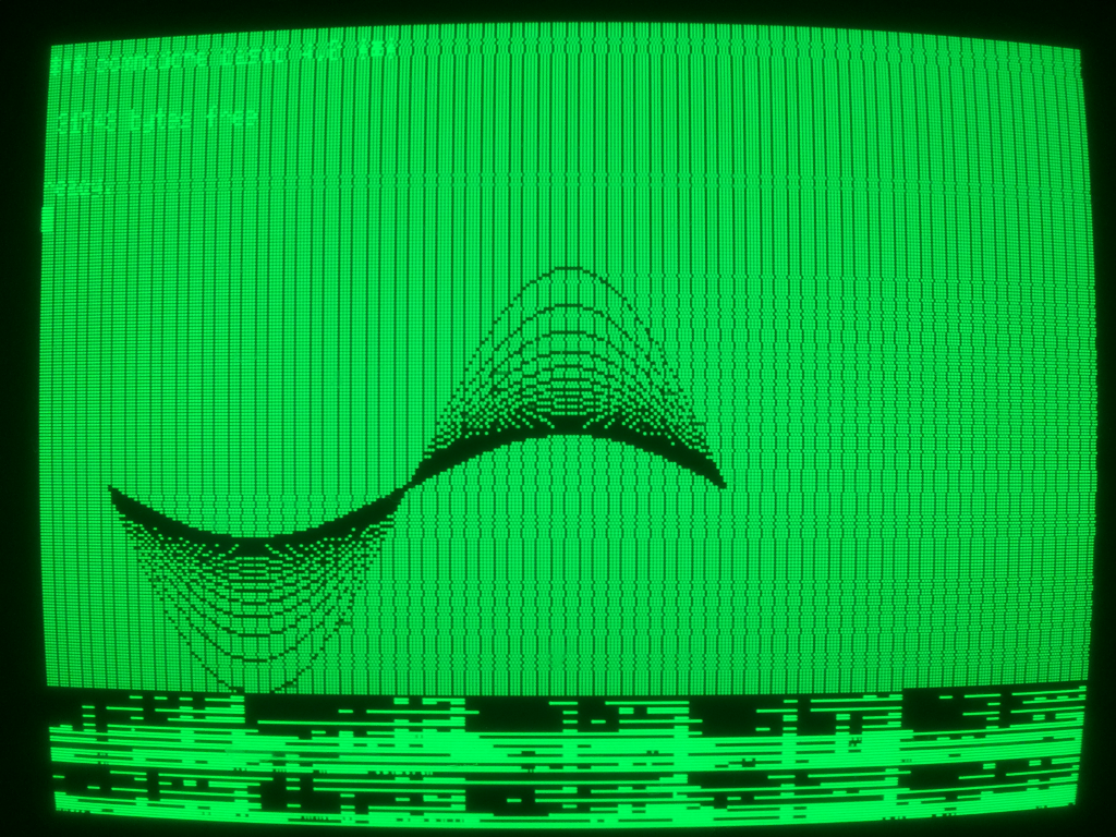
After some time of debugging the sinewaves appeared in a more pleasant fashion:
Men are like little kids so I played with my new toy: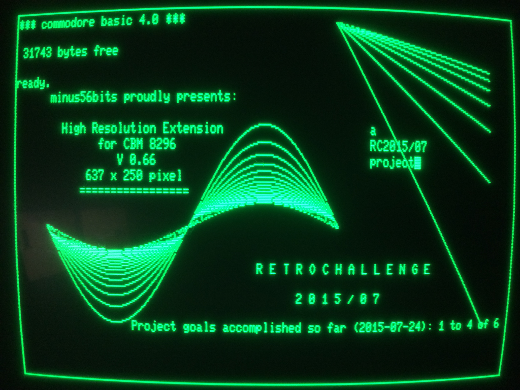 Border, lines and sinewaves have been computed by the HRE microcontroller. Text has been typed on the CBM keyboard. Due to the fact that the HRE has a separate video memory one can type and edit text/programs as usual without destroying the graphics. Current resolution is 637 x 250 pixels. Hopefully an additional debugging session will find the lost three pixels per line.
Implementation of the userport interface will be next. Stay tuned!
RC 2015/7 – Dances with Bits #2
Engineer’s Log, Labdate 0720.23. The Klingons wonder how we manage to stay combat-ready even if they prevent us from getting any sleep. I instructed McCoy to brew up some more of our secret weapon and to hand thermos out to the entire crew.
Yeah! After a slight hardware modification the HRE firmware can now display vertical lines that are aligned  with CBM characters. Nothing to write home about but every little counts.
Vertical synchronisation will be next. Unfortunately I forgot to arrange for VSYNC detection. Oops! There is no pin with interrupt support left. Swapping PE0 / PD0 might help but that’s a task for tomorrow.
And I’ll hunt the jitter down … tomorrow.
Need some sleep badly…
RC 2015/7 – Dances with Bits #1
Engineer’s Log, Labdate 0719.21. Mr. Spock remarks that our computer underperforms even the human brain. That’s nice to hear.
I already had a look at LunaAVR about a year ago but haven’t used it for a real project until now. That’s simply because I haven’t worked on a private microcontroller project last year. LunaAVR has a nice IDE and comes with more than 300 pages of documentation as well as many example programs. There seems to be a small but informed and responsive community. After all it might be the right tool for the job.
Last night I tinkered a bit with the new release. It still lacks support for the external memory interface that I want to use. No big deal, though. Flipping some bits should turn XMEM on (it’s an Atmel term for eXternal MEMory) and memory access will be handled by assembler anyway.
Where do we start? The CBM 8296 should behave as usual until a special command is issued to activate the HRE. For that purpose we have to set pin 9 of the shift register (output) to high level and pin 1 of the multiplexer (A/B switch) to low level so that only the CBM video signal is routed to the monitor. A 10k pulldown resistor takes care of the multiplexer but the shift register has no tri-state output and therefore the microcontroller must initialize the chip. While we’re at it: a subroutine for switching three video modes (CBM only / HRE only / both) would be nice.
Video synchronisation will be next.
IF you haven’t tinkered with video signals
THEN you might find the following (greatly simplified) abstract of avail
ELSE skip next four paragraphs
The CBM has a CRT (Cathode Ray Tube) monitor that sends an electron beam onto a fluorescent screen. The electron beam moves continually across the screen area in a fixed pattern starting at the upper left corner. It then moves horizontally to the right screen border, then back to the left border and down by the width of a pixel. This movement repeats until the beam reaches the bottom right corner of the screen. It then moves back to the upper left corner and the whole process starts again. In other words, the beam moves from left to right and line by line from top to bottom – just like you move your eyes while reading this text.
Three digital signals control the beam. In this text they are labeled VIDEO, HSYNC and VSYNC. One can’t see the beam as long as VIDEO is HIGH. If VIDEO is LOW then the fluorescent coating lights up at the current position of the beam. If HSYNC (Horizontal SYNChronisation) is HIGH the beam passes from left to right along the screen. If HSYNC is LOW the beam moves one line down and back to the left. HSYNC is like Carriage Return and Line Feed for the beam. While VSYNC (Vertical SYNChronisation) is HIGH the beam moves down the screen line by line. The beam returns to its home position (upper left corner) when VSYNC is LOW.
How do we display useful information? By precisely controlling the LOW periods of VIDEO. A long LOW period gives a long horizontal line and a short LOW period gives a short line. Our horizontal timing reference is the 16 MHz pixel clock of the CBM system. 16 Mhz pixel clock means that a single pixel has a duration of 1 / 16,000,000 s = 62.5 ns. Let’s assume we want to display a horizontal line of 8 pixels width. We then need to drive VIDEO LOW for 8 * 62.5 ns = 500 ns. A complete set of pixel information that can be displayed on the screen at a time is called a frame. The vertical timing reference is called frame rate (or refresh rate). It tells us how many frames per second will be displayed, that is how many VSYNC pulses occur per second. My CBM system uses a frame rate of 50 Hz.
Back in the days most computer monitors had quite simple (aka cheap) circuits inside. This tended to result in performance variations within a production lot and in temperature dependency of the display. Imagine they would have used the whole screen area to draw pixels and the start position of the beam moves slightly to the left while the monitor heats up. Some pixels would disapear behind the chassis of the screen. Thus borders were introduced to the timings.
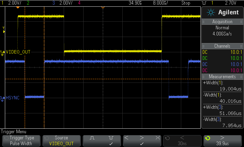 This oscillogram shows a line of 640 bright pixels between two HSYNC pulses. The LOW period is 40 µs which is just what we expect (40 µs = 40,000 ns; 40,000 ns / 640 = 62.5 ns; 1/62.5 ns = 16 MHz). The HIGH period of 19 µs forms the horizontal borders. It takes about 16 µs from HSYNC going LOW to VIDEO_OUT going LOW and about 2.9 µs from VIDEO_OUT going HIGH to HSYNC going LOW. These periods define the horizontal position of the visible area.
To synchronize the HRE output with the CBM output I’ll use an interrupt that is triggered by HSYNC. Due to the fact that we have to be cycle exact in our timing we must take interrupt latency into account. The ATmega completes any ongoing instruction before an interrupt can be serviced. Since execution times vary from 1 to 4 cycles per instruction, an interrupt service routine has a random entry time. The solution to this problem is to put the µC into sleep mode. It then always executes the exact same steps when it wakes up and these will take always the exact same time to execute.
RC 2015/7 – Off Topic
Looking for debugging fun? How about this: Connect the RESET line of your microcontroller to an output pin that occasionally changes its level.
Yep. I’ve been there. Don’t ask me why. Maybe sunstroke while soldering. So much for “Hardware has no severe faults.”