Any home computer needs at least an input device, a computing device and an output device. I plan to use a keyboard as input, an ATmega1284 microcontroller with some external SRAM as the computing device and a VGA display as output.
I happen to have a working VGA color graphics circuit (as a result of my RC 2017/10 entry) that I’m going to recycle for this home computer project. First step is to compress its breadboard footprint:
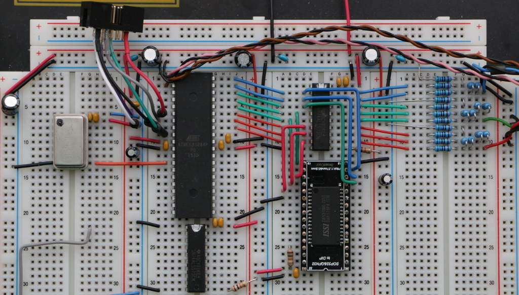
Main components from left to right:
– 25 MHz TTL oscillator
– top: ATmega1284P microcontroller, bottom: 74ALS573 latch
– top: 74ALS573 latch, bottom: IS61C5128AS 512K x 8 25ns SRAM
– 21 resistors (560 ohm) forming 3 digital to analog converters
plus several capacitors and pull up/pull down resistors.
Meaning of wire colours:
– black: ground
– red: supply voltage (+5V DC) or data lines for the red color path
– green: data lines for the green color path
– blue: data lines for the blue color path
– orange: system clock (25 MHz)
– purple: address lines A0, A1, A2
– grey: address lines A3 to A10
– white: address lines A11 to A18
– yellow: control lines (like chip enable, output enable, …)
– pink: horizontal sync
– brown: vertical sync
To be honest, I’m violating rule #1 here: The external SRAM is a SMD chip on a breakout board. I simply couldn’t find any DIP SRAM with an access time of 40ns or less. The RC2017/10 project successfully used a 55ns chip well beyond its specifications, but only when wired in a special way. The MCU is also overclocked (max. clock speed 20 MHz specified) but it runs easily at more than 30 MHz, so I consider 25 MHz to be save.
Adding wires for address lines…
Ok, I need something to eat now, so I’m going to declare this circuit to be the minus56 home computer, version 0.01 alpha. 😉
Moderated comments are used to prevent spamming,
so it’ll take some time
before your comment gets published.
I just found your page via a post on Google Plus. Interesting project!
Instead of the “cheat” with the SMD SRAM chip, you could use the Alliance 7AS256B. It’s available in 28 pin DIP with 5V power supply and 15ns(!) access time. But unfortunately it’s only 32KB, not 64KB so you’d need two of those for the same amount of space, plus a little bit of logic (probably just an inverter gate, I haven’t looked at your schematic yet) to enable just one of the two depending on the address.
https://www.mouser.com/_/?Keyword=AS7C256B&FS=True
There may be other SRAM chips by Alliance that might be of interest. I can’t think of the type right now but they even have a 512KB (yes kiloBYTE) SRAM chip in DIP package. I’m not affiliated with them by the way.
Thanks for your hint, Jac! Unfortunately a single frame needs 307.200 bytes (640 x 480 pixels @ 256 colours), which translates to 10 of these 32KB chips. In fact I’m using even more RAM per frame due to the memory layout in the firmware. I’ve been using several 512KB-55ns SRAM chips in DIP packages. They worked fine at 40ns and 20°C as long as subsequent reading cycles did access different colums of the chip. I’ll go with the SMD chip for RC2018/04 to avoid the additional wiring but will consider the 32KB DIP chips for a prototype PCB.