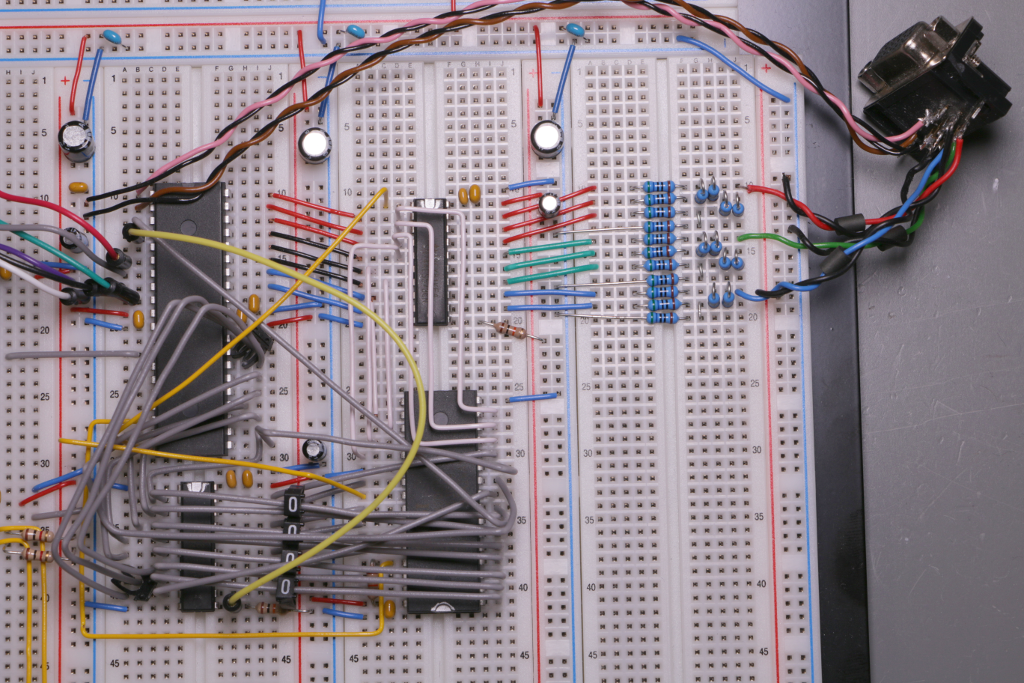
Now that the graphics circuit seems to work, I should give you an overview of the current state of the hardware. Please match this picture of the breadboard
with this
The position of the components on the breadboard is roughly reflected in the circuit diagram.
VGA synchronising is handled by PB0 (horizontal sync, pink wire) and PB1 (vertical sync, brown wire).
Latch U2 separates the pixel data bus (Color0..7) from the digital to analog converter during the blanking periods when the microcontroller sends pixel data from Port A to the SRAM. U2 is controlled by PD6. SRAM read/write mode is controlled by PD4.
The address bus is partly multiplexed. PB2 selects the most significant address bit (Addr18). PB3 switches latch U3 into transparent mode, then Port C puts address bits 10 to 17 on the bus, then PB3 switches U3 into latched mode, then Port C puts address bits 2 to 9 on the bus and PD7 / PD5 deliver Addr0 / Addr1.
While streaming pixels from SRAM to the screen Port A is in high impedance state and U2 in transparent mode. Three simple R2R resistor ladders convert the digital color information into analog voltages. Eight shades of red, eight shades of green and four shades of blue make 256 colors in total.
I haven’t decided how to connect to the PET yet. I would like to utilize a shift register in the 6522 interface chip as I have two serial ports available on the ATmega, but unfortunately the 6522 has at least one major bug. From what I’ve read so far it seems that the error only occurs when an external clock is used. Exhaustive tests have to be performed, I’m afraid. Time to play with the EEs best friend… 😉