RC 2018/04 – Final Post

Oh dear! Almost no time led to absolutely no blogging about nearly no progress. I call that a non-starter in RetroChallenge terms.

What does ‘nearly no progress’ mean? Well, the VGA circuit has been rearranged and the firmware has been restructured to free a few cycles. Hopefully. Tests required. It still supports full color graphics at a resolution of 307.200 pixels (640*480) and a color depth of 8 bit (256 colors per pixel).

What’s next? Most likely I’m going to work on the sound circuit. The only musical instrument that I master halfway is the morse key, so it might be fun to watch me while I’m trying to develop a sound card. 😉

Moderated comments are used to prevent spamming,
so it’ll take some time
before your comment gets published.

RC 2018/04 – The minus56 home computer

What if personal computers wouldn’t have displaced home computers?

What if the number of software abstraction layers wouldn’t have exceeded the number of CPU pins?

What if the time to market had not been favoured over flawlessness?

Don’t panic! I don’t want to start several flame wars in parallel here. I just lack a justification for another crazy project and these questions should confuse people so that they don’t ask why (aka Captain Jack Sparrow Principle): I’m going to build a home computer from scratch – just for the heck of it. Nothing like the boring Pi + Linux + WallpaperOfMyCat stuff and unfortunately nothing like the awesome MOnSter 6502 <kneel down>. It’ll be something in between.

So, what is my conception of a home computer?

1. based on electronic parts available to mere mortals
2. modular, expandable and (hopefully) easy to understand design
3. colour graphics and sound
4. SD card storage
5. integrated operating system and programming language
6. favour flawlessness over featuritis
7. good technical documentation

Given the limited time, what are my goals for this RetroChallenge?

I’m toying with the idea to build a computer from scratch for ages.  “No time for a project of this dimension” has been my excuse all the time. Essentially, that’s true. So, what is the point of a never ending story? Well, the journey is the reward.

Seriously, there is only one goal: To get this project started!

The above list is pretty vague. So, let’s concretise:

1. Leaded components only, as I love prototyping on breadboards. As few different components as possible. As few special / highly integrated hardware as possible. All components must be available in single digit quantities.

2. Each function module in a separate circuit block. For example, video controller and sound controller will reside on separate MCUs, even if they would easily fit into one.

3. You don’t expect a home computer without graphics or sound, don’t you!!!

4. SD cards are common, cheap, robust and fairly easy to connect, so why not?

5. That’s a difficult one. I want a home computer with batteries included, but developing an operating system, an editor and an interpreter/compiler isn’t precisely a trivial task, even if the functionality would be fairly basic. Let’s discuss this topic when the hardware is already running…

6. This is a hobby project, so I don’t have to worry about marketing. I appreciate any serious suggestion (well, most likely I’m the only nerd who enjoys this kind of endeavour, but in case you happen to be my twin from another universe, please feel free to join the adventure and give me a shout at universe42.galaxy484027.solarsystem925482537.planet3.hominids. globalcom.twitter.username: @minus56bits), but won’t implement features just for the sake of another NEW sticker.

7. Yeah, ok. You already know that this isn’t going to happen, don’t you. At least not in the course of this RetroChallenge. The idea is to support people who would like to get into embedded systems. One can certainly argue about whether the term ’embedded system’ is appropriate in this context, but in my opinion programming is ’embedded’ as soon as you do it on the bare metal.

Ok, heading over to the breadboard…

Moderated comments are used to prevent spamming,
so it’ll take some time
before your comment gets published.


RC 2017/10 – Final Post #2

It’s been great fun to work on this project  in the course of the RetroChallenge! As always, free time was the limiting factor, but I’m quite happy with the result. My beloved PET turned into a machine that would have been a high res color workstation in the 70s. Well, granted, 8 kB of RAM and 1 MHz clock wasn’t that much for a workstation even back in the day, but together with the 512 kB framebuffer RAM of the CHRE and its 25 MHz GPU it’s a real beast, isn’t it? 😉

All of my initial goals have been achieved, with the exception of a BASIC extension. I had the hardware of the 8xxx series in mind when I wrote this goal up. Unfortunately the PET doesn’t have ROM extension sockets, so I ditched this goal and went with a simple machine language subroutine located in the cassette tape I/O buffer. Yes, the PET does have an expansion port and, as the name implies, it’s possible to add ROM this way, but that would have been a RetroChallenge on its own.

But I’ve been a lucky fellow on another topic: resolution. To be honest, I adopted a widespread beliefe on the internet that it would be  impossible to put out a resolution of 640 by 480 at 256 colors with an ATmega microcontroller, some SRAM and two latches. It was a pleasant surprise to bump into a viable solution anyway. Granted, it’s open to dispute if it makes sense, but it’s definitely possible! It is said that the judges look out for some silly things. Here you go! 🙂

I have struggled with video and pictures this time: too flickery, too bright, too dim, incorrect colors, reflections, bad sound and so on. It took me much more time to do the video than to write the demo program, to say nothing of the extreme lame data rate while uploading the video. So, there is room for improvement and a lot to learn until the next RetroChallenge.

My to-do list (aka list of reasonable or silly features) seems to increase each time I work on this project. Sounds familiar? Proposed solution?

K E E P    O N    R E T R O C H A L L E N G I N G !

Thank you for your interest! Please stay tuned (Twitter: @minus56bits).

RC 2017/10 – PET Comm #4

Originally I wanted to put all machine language routines into an EPROM at one of the ROM expansion sockets, but in contrast to the PET 8000 series the PET 2001 has no ROM expansion sockets. Fortunately, it has 6540 ROMs which cannot be substituted by ‘modern’ 27xx EPROMs. ‘Fortunately’??? Yes, because this prevents me from patching the Kernal and/or BASIC ROMs.  😉

Next resort are the cassette tape I/O buffers. Last winter I bought a SD card mass storage device for the PET series, called petSD+ (designed by Nils Eilers). It connects to the IEEE 488 port and pretends to be a floppy drive, so I don’t depend on a tape drive anymore.
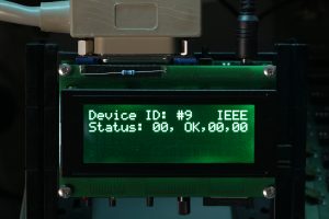
Off topic: Honor to whom honor is due. I bought my petSD+ from Dave Stevenson, who is one of the most kind and cooperative guys I’ve met on the internet. Thanks again for your great support, Dave!  🙂

The PET series supports two tape drives, each of which has an associated RAM buffer of 192 bytes (tape I/O buffer #1  $027A – $0339; tape I/O buffer  $033A – $03F9). Just for the record: Without intending to appear ungrateful I would like to point out that 384 bytes really isn’t a giant amount of RAM, thus I’ll start with a basic version of the API and maybe add convenience later – at the expense of BASIC RAM.

This is my preliminary solution: Three integer variables are reserved for parameter passing. These variables must be assigned before any other variables are used in the BASIC program and they have to be assigned in a specific order! The ML subroutine expects to find the parameters in the order ‘drawing instruction’ [0..63], ‘parameter #1 [0..639]’, ‘parameter #2 [0..479]’ at the start of the variables in memory. Example:

0  REM ###         CHRE SETUP        ###
1  REM ###   DO NOT MODIFY !    ###
2  DI%=0 : P1%=0 : P2%=0
3  REM ### END OF CHRE SETUP ###

The subroutine doesn’t care about variable naming, so someone might use this

2  Z6%=0 : BT%=0 : A%=0

Warning! Doing this may have serious side effects such as long-lasting headaches!

To command the CHRE we need to assign appropriate values to the variables, then call the subroutine. The following example positions the graphic cursor at X=321, Y=290:

1000  DI%=3 : P1%=321 : P2%=290 : SYS 635

Granted, that’s not as elegant as

1000  GCURSOR (321, 290)

but it does the job.

A BASIC integer variable is stored in 7 bytes. Bytes #0 and #1 contain the name and type of the variable, byte #2 the MSB and byte #3 the LSB of the 16 bit value. Bytes #4 to #6 are not used. Yep, Billysoft looks back on a long tradition of wasting RAM. BASIC stores a pointer to the start of the variables at address 42/43 ($2A/$2B). Please note that variables are stored in sequence MSB/LSB and pointers are stored in sequence LSB/MSB. Yep, Billysoft looks back on a long tradition of confusing people, too.

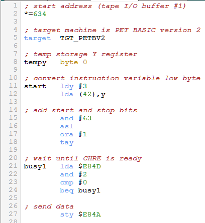
Let’s take a look at the source code:

Lines 11-12: The subroutine’s entry point is labeled ‘start’ (address 635 / $027B). Indirect indexed addressing is used to fetch the LSB of the first variable (aka drawing instruction).

LSB
ddddddd

Lines 15-18: We mask bits #6 and #7, shift left by 1 and add 1 (aka add start and stop bit):

LSB                                   63                  RESULT
xxdddddd    AND    00111111    =>   00dddddd

LSB                                                         RESULT
00dddddd     ASL                          =>   0dddddd0

LSB                                     1                  RESULT
0dddddd0    ORA     00000001    =>   0dddddd1

Backup result in register Y.

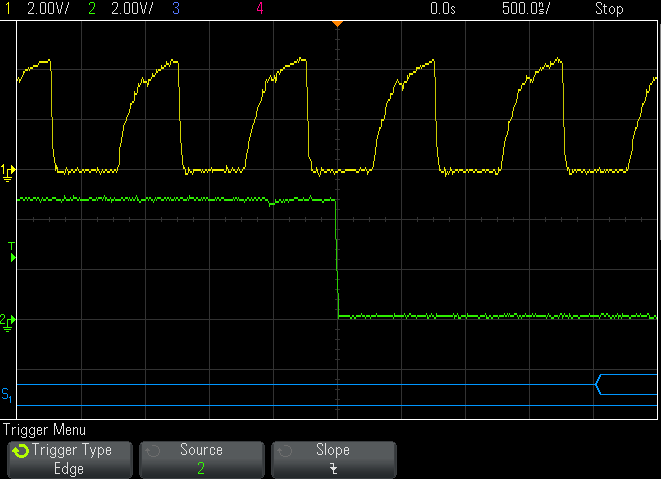
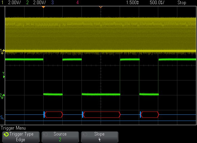
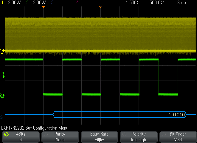
Lines 21-24: Serial communication is a low priority task on the CHRE side, so we have to check if CHRE is ready to receive before we start the transmission.

Line 27: Data is transfered to the shift register. Shift out starts immediately.

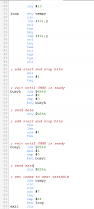
Line 29: We ignore the MSB just to show Goliath that David can waste even more RAM and set the index to LSB of the second variable (aka parameter #1).

Lines 31-34: Now we have to deal with values up to 639, thus we need to convert into two 6 bit values. Accumulator, register Y and register X will be used, so we backup the index value first. Then we clear the carry flag, as we are going to rotate through carry. Indirect indexed addressing is used to fetch the LSB of the second variable (aka parameter #1). Rotate left through carry:

C    LSB                                   C     RESULT
0    dddddddd    ROL    =>    d    ddddddd0

Lines 35-38: Backup result in register X. Set index to MSB. Fetch MSB of the second variable (aka parameter #1). Rotate left through carry:

C    MSB                                  C     RESULT
d    XXXXXXDD   ROL    =>   X    XXXXXDDd

Lines 39-41: Backup result in register Y. Restore intermediate state of LSB conversion. Rotate left through carry:

C    LSB                                   C     RESULT
X    ddddddd0    ROL    =>    d    dddddd0X

Lines 42-44: Backup six-bit LSB in register X. Restore intermediate state of MSB conversion. Rotate left through carry:

C    MSB                                  C     RESULT
d    XXXXXDDd   ROL    =>   X    XXXXDDdd

Lines 47-49: Do you remember?

MSB                                                          RESULT
XXXXDDdd     ASL                          =>   XXXDDdd0

MSB                                     1                    RESULT
XXXDDdd0     ORA     00000001    =>   XXDDdd1

Line 48a: At this point the developer realizes that he missed to mask bits #6 and #7. Bad for his ego, but great to check if John really reads all this. Assume that the developer will insert an AND #63 here.

Lines 52-58: As stated in the comments and discussed above.

Lines 61-64: Restore six-bit LSB. Logical shift right:

LSB                                                         RESULT
dddddd0X    LSR                           =>   0dddddd0

LSB                                     1                  RESULT
0dddddd0    ORA     00000001    =>   0dddddd1

Backup result in register X.

Lines 67-73: As stated in the comments and discussed above.

Lines 76-82: Restore index and add 7 to point to the next variable. If index is not equal to 24 goto label ‘loop’.

Line 83: Make an educated guess!

Any 6502 guru reading this? I’d like to hear from you! How can this subroutine be optimized? TIA

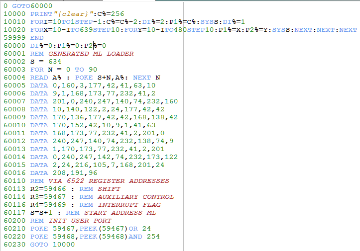
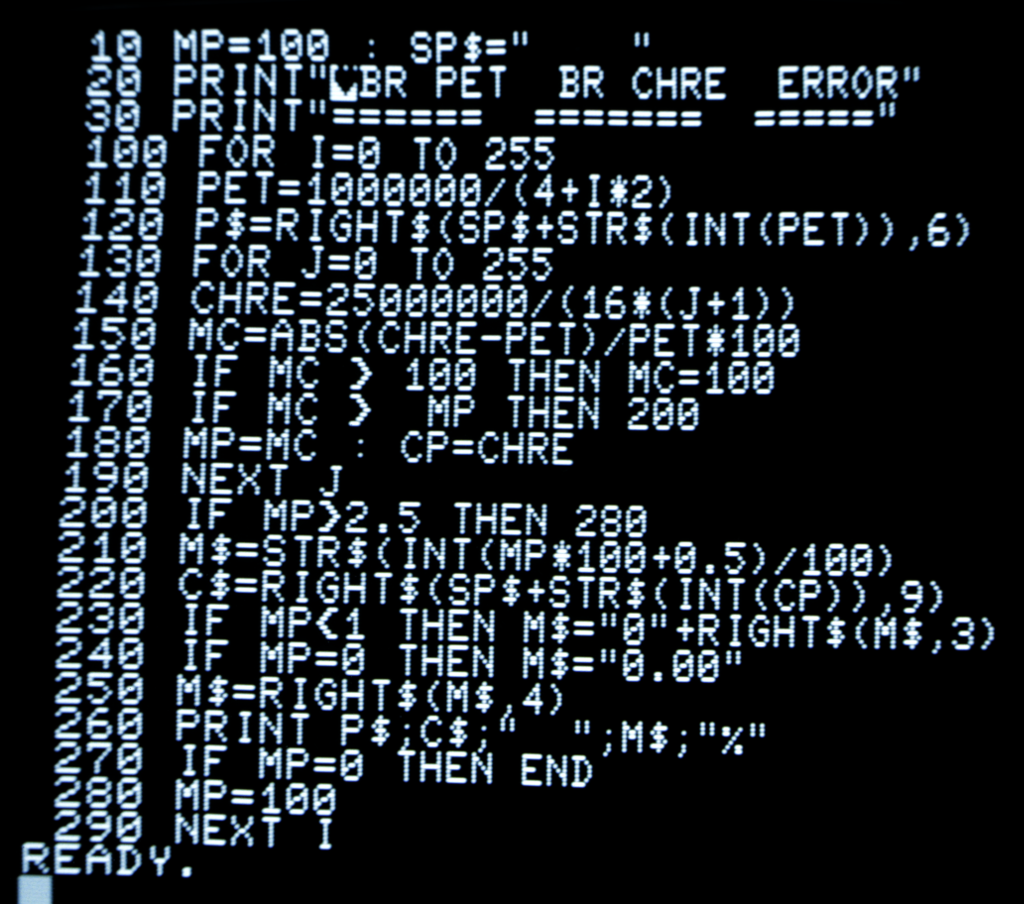
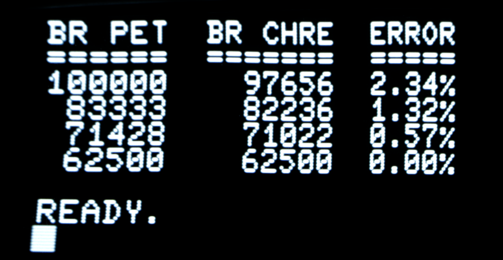
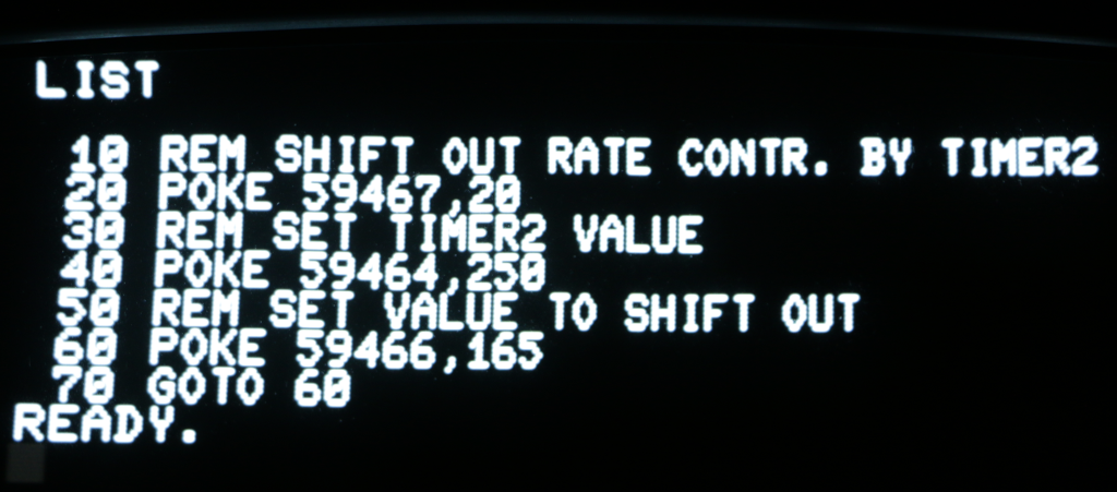
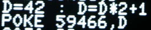
The following BASIC program is used for the performance test. I compressed several statements into a line and removed any spaces to make it as ugly as possible – and to squeeze out the last ounce of performance, but apart from that it should be quite self-explanatory.

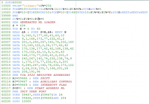
This BASIC program as well as the machine language subroutine have been programmed with CBM prg Studio (designed by Arthur Jordison). Thank you very much for providing this software to the community, Arthur!

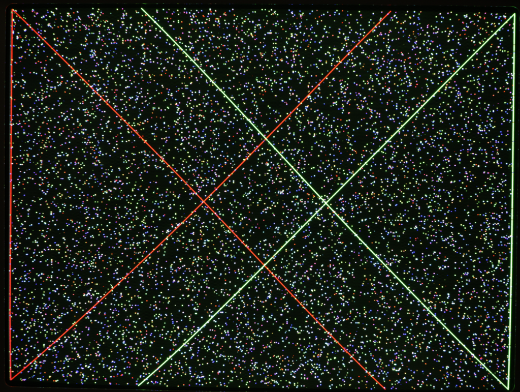
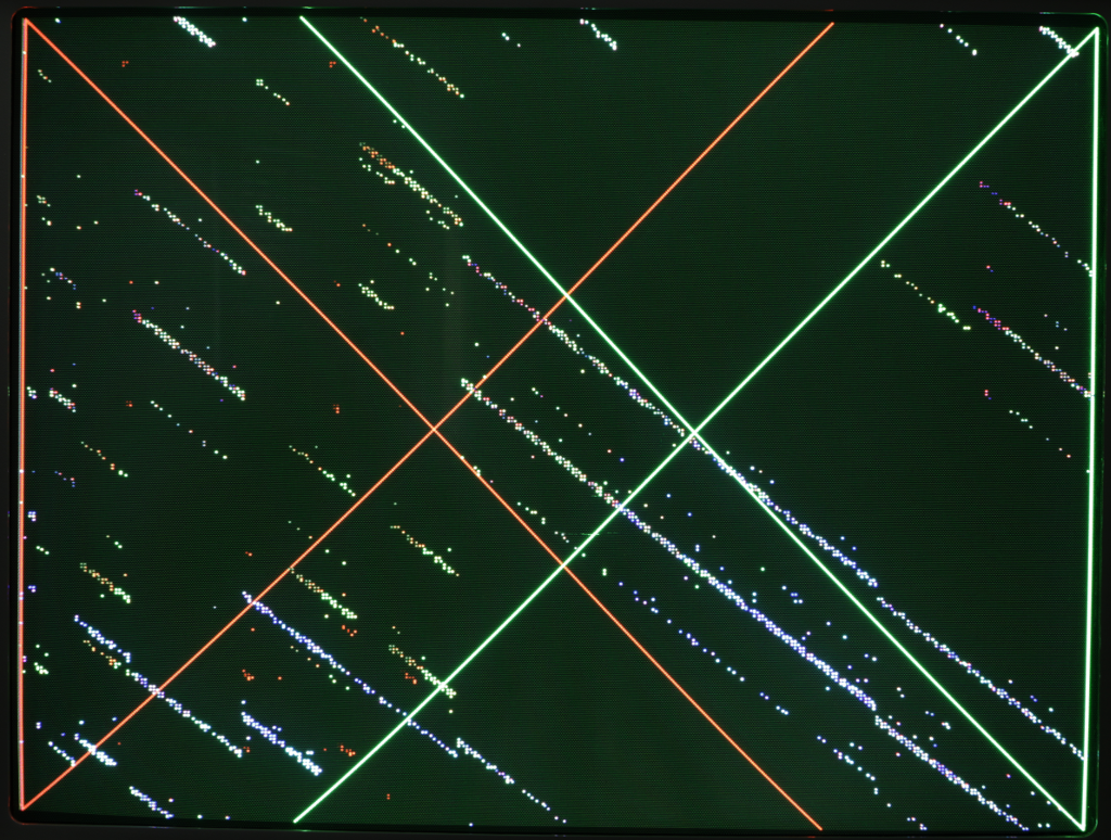
Currently SetColor, PositionCursor, DrawPixel and PrintCharacter are implemented in the CHRE firmware and seem to work. No serious testing done, yet. DrawLine implementation is work in progress (aka it stinks)…
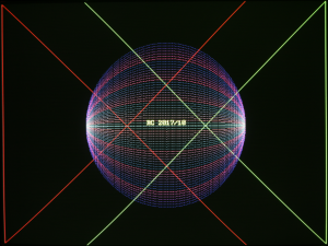
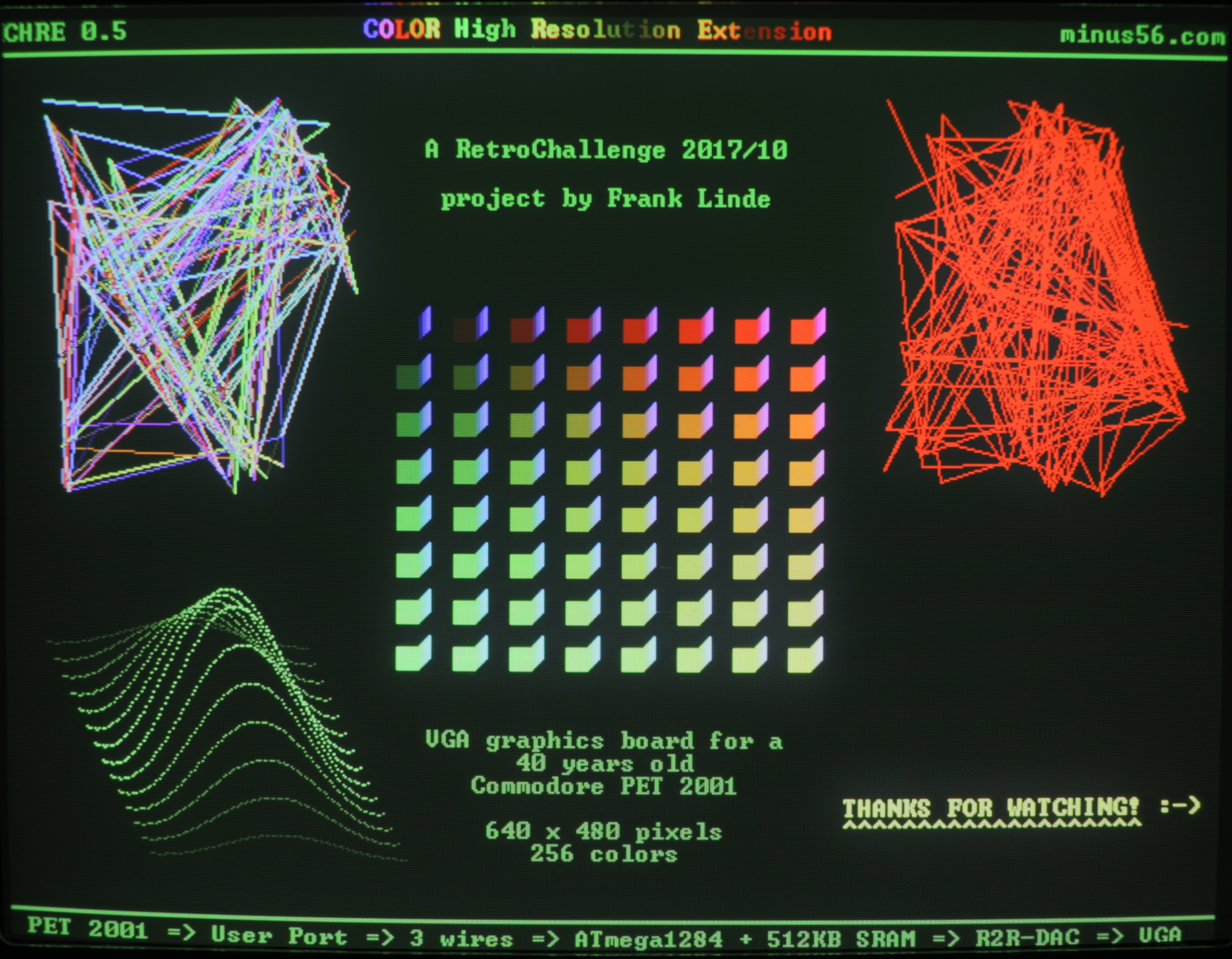
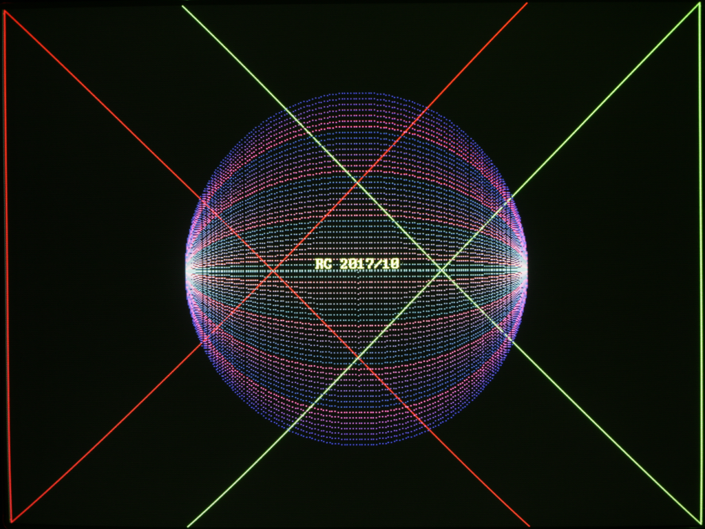
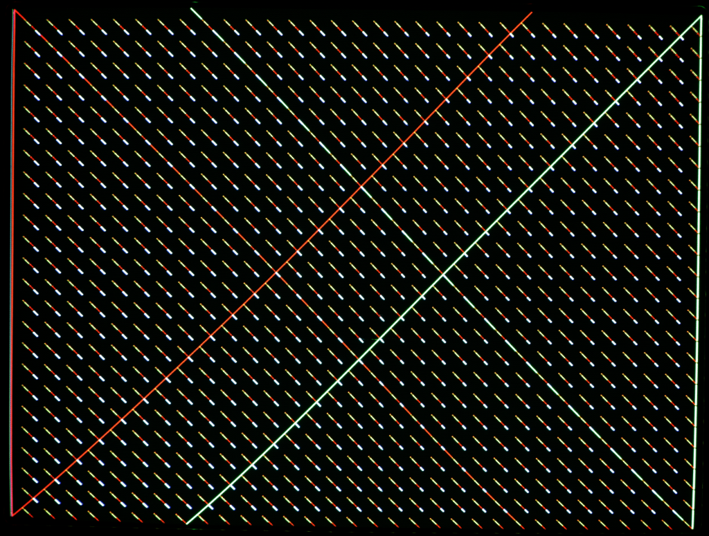
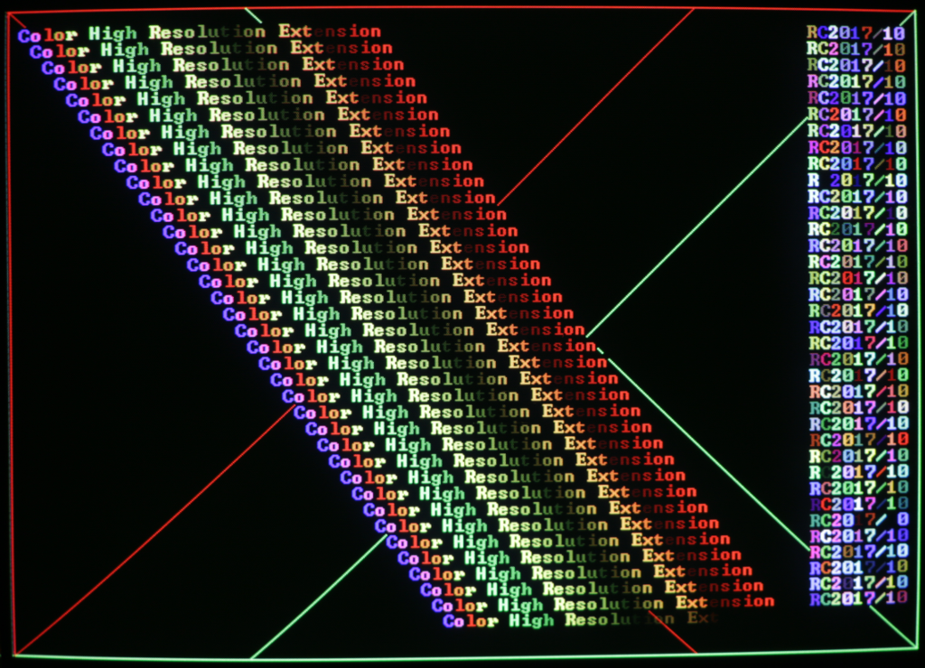

RC 2017/10 – PET Comm #3

Just to make sure the protocol is okay, a small BASIC program sends six frames of data per pixel representing X coordinate, Y coordinate and Color. It’s easy to convert the values into 6 bit wide words:

Xhigh = INT(X/64) : Xlow = X-XH*64      (  X [0..639]  )
Yhigh = INT(Y/64) : Ylow = Y-YH*64      (  Y [0..479]  )
Chigh = INT(C/64) : Clow = C-CH*64      (  C [0..255]  )

Data is sent in the order Xhigh, Xlow, Yhigh, Ylow, Chigh, Clow. There is no function identifier transfered to keep it as simple as possible for the moment. Therefore the CHRE executes always the SetPixel(x,y,c) function to draw a single pixel at the coordinates x,y in the color c.

The following image shows some red and green lines that are coded into the CHRE firmware. This test pattern is written to the framebuffer when the CHRE is ready to receive serial data. The colorful small lines that are evenly spread are drawn pixel by pixel of the received data packets:

I’m very happy with the result. No missing pixels, no pixels out-of-line.

It took ages to render this image at a rate of 5 to 6 pixels per second. That was to be expected, though. BASIC is way too slow for this task. For the final version I’ll write all communication related code in Assembler.

By the way: Have you ever wondered why some of your BASIC games were pretty predictable despite the fact you used the random number function? Well, I did back in the day! The next picture shows random pixels:

And this picture shows random pixels, too:

Both BASIC programs were identical, with the exception of the parameter for the random number function: RND(1) vs. RND(0)
All necessary information was in the manual of the 8xxx series, but as far as I remember we never had a PET 2001 manual in school. Maybe our teacher hid the manual to hold all the cards? Pointless! 🙂


RC 2017/10 – PET Comm #2

When trying to communicate over a serial link, it’s essential to make sure that both sides use the same bit rate. Usually a small mismatch is allowed, depending on the ‘intelligence’ of the involved circuits, but we strive for a 100% match to get the most reliable connection.

In our case, both devices are dividing the system base clock by a specific factor to define a bit rate. These factors are integers, therefore we can not always do an exact division of the system frequency to get the bit rate wanted.

We’ve seen in a previous post that the PET’s highest bit rate (under control of timer 2) is 250,000 bit/s. Of course we’d like to use this bit rate for best data throughput. The ATmega1284p datasheet specifies the following equations for calculating the bit rate and for calculating the value for the USART Baud Rate Register (UBRR):

UBRR = system clock frequency / (16 * BAUD) – 1

BAUD = system clock frequency / (16 * (UBRR + 1))

To get the desired 250,000 bit/s we must set UBRR to

25,000,000 / (16 * 250,000) – 1 = 5.25

The integer closest to this real is 5. Now we double check:

BAUD = 25,000,000 / (16 * (5 + 1)) = 260,416.6667

Oops! That’s more than 4.1 percent off! According to the datasheet, the maximum baud rate error must not exceed +/-2.5 percent. So, our next job is to find the highest bit rate where the mismatch is less or equal to 2.5 percent. Now the PET’s number crunching power comes in handy:

Programmed on the real hardware. For small BASIC programs that’s still ok (kind of), but for Assembler I will switch to CBM prg Studio and VICE!

These are the highest bit rates:

62,500 bit/s is four times slower than what we hoped for. Anyway, that’s the bit rate to start with. If the software on both sides of the serial connection is running flawlessly, we may try the other three rates…

RC 2017/10 – PET Comm

I had a nightmare last night. The oscillogram of the phase2 clock (see previous post) turned into a nasty saw and cut the mainboard of my PET in half. I definitely should go and find the cause of this weird thingy that pretends to be a rising edge, but that investigation might take a while longer. To get on with the main project, I’ll mimic the PET’s own pragmatic way for a moment: Ignore! Business as usual!

Now that we have found the 6522 shift register working even at high speed, it should be suitable to transmit data to the CHRE. The PET also needs a way to check if the CHRE is ready to receive (more) data. We add a binary busy/ready signal and end up with a three wire connection:

PET userport pin 11 <—-> CHRE ATmega pin 11, GND, black
PET userport pin M,   —-> CHRE ATmega pin 14, DATA, blue
PET userport pin B,  <—-   CHRE ATmega pin 15, BUSY, yellow

Have you ever experienced the resolution cancellation phenomenon? No, I’m not talking about politics here. What I mean is: You start with the intention to write a serial communication protocol, but get distracted by some other code as soon as your IDE pops up? I went down the rabbit hole of performance optimization. Yes, I know the rule. Don’t optimize your code in an early stage! I just couldn’t resist.

To make a long story (aka coding&debugging session) short: The time to produce this demo output

has been reduced from 10 minutes to 16 seconds. That’s still slow as a snail, but now it’s a snail on amphetamine! 😉

Provided that I did count accurate, the screen content is built up of 153,728 pixels. 153,728 pixels divided by 16 seconds equals 9,608 pixels per second. Back to serial communication: Drawing a single pixel is the most basic function the CHRE has to provide. And it’s the worst case in terms of the communication protocol as well: Only one pixel per function call. How many DrawPixel function calls can we transfer over the serial link at a bit rate of 250 kbit/s ?

A serial frame consists of one start bit, six data bits and one stop bit. Without further encoding, we would need seven frames:

1 frame function identifier (using 6 bits),
2 frames X coordinate (using only 10 bits out of 12),
2 frames Y coordinate (using only 9 bits out of 12),
2 frames color (using only 8 bits out of 12).

These seven frames correspond to 56 bits (start and stop bits included). So we can transfer 4,464 frames per second (250,000 divided by 56). That’s insufficient, isn’t it? Well, it depends.

The CHRE pixel rate is already very slow. The ATmega is currently using nearly all of its processing power to handle the framebuffer and do the rendering. We’ll have to steal some clock cycles from the rendering to implement a serial protocol, hence reduce the amount of pixels the CHRE can render per second. Another aspect is the real application. A few thousand pixels per second may be adequate if the PET does analysis of a math function and curve sketching. A 3D ego shooter is out of reach, though.

Coding time…

RC 2017/10 – 6522 inspection

In addition to the IEEE-488 bus the Commodore PET/CBM series features an 8-bit parallel interface named Userport. A single 6522 Versatile Interface Adapter (VIA) provides bidirectional I/O lines, two 16-bit timers and an 8-bit shift register for serial communications.

The monochrome High Resolution Extension (RC 2015/07) used a parallel protocol for Userport communication. In theory we could use it with CHRE as well since there are eight free I/O pins left on the ATmega (four pins of the programming header included). But I hope to keep a few extra clock cycles on the ATmega if I use its USART (Universal Synchronous/Asynchronous Receiver/Transceiver) hardware support for serial communication.

Only a few cycles? So why bother about it at all? Well, lets compare the requirements:

HRE:
resolution 640 by 250 pixel
one BIT per pixel (monochrome)
20,000 bytes per frame
50 frames per second
data transfer rate about   1 MByte per second

CHRE:
resolution 640 by 480 pixel
one BYTE per pixel (256 colors)
307,200 bytes per frame
60 frames per second
data transfer rate about 18 MByte per second

The CHRE microcontroller is somewhat more stressed due to this tiny difference. It has to spend a lot more processing power on the job. This leaves us with only a small amount of time to

  • do PET communication,
  • decode, verify and dispatch the received drawing commands,
  • do the rendering.

For example, it took nearly ten minutes (!) to render the screen content that I posted the other day. Granted, there is room for firmware improvement, but it definitely makes sense to be picky about the use of clock cycles.

It is said that the 6522 VIA shift register will lose a bit if an externally supplied shift clock edge falls within a few nanoseconds of the falling edge of the internal clock. So maybe the shift register won’t bug me if the internal I/O clock is used?  I’m sure there is a comprehensive discussion about this issue somewhere on the internet, but I couldn’t find it. Oookay, you’ve got me! I’ve done no more than a superficial search, because I’d like to play with the scope. The official statement is: I need to know if the VIA in my PET is functional at all. 😉

We don’t have to comply with any standard here, so we start the test with a bit rate of 2,000 bit/s. The VIA setup is done by a short BASIC program:

Let’s look at the clock signal first:

Ch1:  internal I/O clock (phase 2)
Ch2:  output shift register (bitstream)
S1:  decoded bitstream (binary)

Ohuuu, that’s not exactly the most rectangular square wave I’ve ever seen, I’m afraid. However, surprisingly the VIA doesn’t seem to care! The bit stream looks quite good at first glance:

Yep, there’s a problem with the second glance: Now you wish you had stuck to the first one. Anyway, we have to note the absence of any decoded data. The empty red boxes are a polite indication that

a) the VIA is really faulty,
b) the creature in front of the scope made a suboptimal decision.

Make an educated guess…

… It’s  b).  Using 8 bit data wasn’t clever.

The shift register in this VIA is just an 8 bit shift register, no complete UART/USART. It does not send a leading start bit and does not send a trailing stop bit either. Without a start bit the scope cannot detect the beginning of a frame and therefore cannot decode the bitstream.

A slight modification to the BASIC program reduces the usable data length to six bits. The answer to all questions is stored in variable D (binary 00101010). We multiply by 2 (result: binary 01010100) and add 1 (result: binary 01010101). The MSB is now zero (aka start bit) and the LSB is one (aka stop bit).

Now the scope decodes the data:

To find out if there is some kind of rare glitch we use the mask test function of the scope:

I’ll call that a promising result. When cranking up the bit rate to 250 kbit/s we get the same good result. So we may assume that at least an unidirectional serial communication is possible…


RC 2017/10 – Schematic

Now that the graphics circuit seems to work, I should give you an overview of the current state of the hardware. Please match this picture of the breadboard

with this

preliminary schematic

The position of the components on the breadboard is roughly reflected in the circuit diagram.

VGA synchronising is handled by PB0 (horizontal sync, pink wire) and PB1 (vertical sync, brown wire).

Latch U2 separates the pixel data bus (Color0..7) from the digital to analog converter during the blanking periods when the microcontroller sends pixel data from Port A to the SRAM. U2 is controlled by PD6. SRAM read/write mode is controlled by PD4.

The address bus is partly multiplexed. PB2 selects the most significant address bit (Addr18). PB3 switches latch U3 into transparent mode, then Port C puts address bits 10 to 17 on the bus, then PB3 switches U3 into latched mode, then Port C puts address bits 2 to 9 on the bus and PD7 / PD5 deliver Addr0 / Addr1.

While streaming pixels from SRAM to the screen Port A is in high impedance state and U2 in transparent mode. Three simple R2R resistor ladders convert the digital color information into analog voltages. Eight shades of red, eight shades of green and four shades of blue make 256 colors in total.

I haven’t decided how to connect to the PET yet. I would like to utilize a shift register in the 6522 interface chip as I have two serial ports available on the ATmega, but unfortunately the 6522 has at least one major bug. From what I’ve read so far it seems that the error only occurs when an external clock is used. Exhaustive tests have to be performed, I’m afraid. Time to play with the EEs best friend… 😉