Engineer’s Log, Labdate 0715.14. We have stopped our engines for maintenance and upgrade. Mr. Scott is supervising the initial startup procedure of the new warp extension.
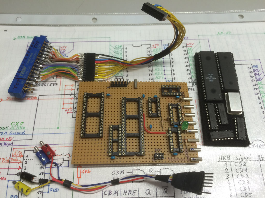 Tadaaaah!!! Here it is: The Double Retro Kit! It’s double retro because it has been built entirely from parts out of my junkbox. 😉 I used my last card connector that fit the CBM/PET boards. In case you know a source where one can still buy these connectors, please drop me a line.
The 1:1 adapter from user port to pin header hasn’t been finished yet. The whole thing will have a bath in epoxy sometime.
WARNING! FOR ADULTS ONLY! AWFUL MESS OF WIRES AHEAD!
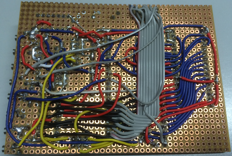 Yep! There are some very good reasons why not to build it like this. We have to handle high-speed digital signals (pixel stream, fast edges of 74AC00 and 74ALS573) and if this project were meant to be a consumer product, a proper PCB would be required. I consider this project to be a proof of concept and hope to get along with the direct wiring. I’m prepared to fix some weird issues that might pop up, though.
Ok, let’s populate the board step by step and do some checking. Maybe we can prevent it from catching fire. Please feel free to skip the rest of this post as it might be quite boring to read unless you are interested in the engineering part of the story (aka watching me putting my foot in my mouth).
Step 1: Limit power supply to 40 mA; check current consumption with empty sockets.
Target: < 1 mA
Actual: < 1 mA (passed)
I’d like to see if the CBM video signal can pass the HRE board without interference. It enters the HRE at pin 2 of the multiplexer (74HC257) and is fed to the NAND (74AC00) afterwards. Let’s check that path.
Step 2: Insert 74HC257; check current consumption and voltages.
Target: < 1 mA
Actual: < 1 mA (passed)
Target: 5.0 V
Actual: 5.0 V (passed)
Step 3: Insert 74AC00; check current consumption and voltages.
Target: < 1 mA
Actual: 4 to 32 mA (failed)
Target: 5.0 V
Actual: 5.0 V (passed)
It seems as if we have some unwanted oscillation here. That’s ok because of currently floating inputs at pin 9 and pin 10. Does the current stabilize if we apply some pulldown resistors? Fortunately, yes. The current drops below 1 mA. (passed)
Step 4: Connect HRE to user port; start CBM; check video signal.
Target: The signal should look quite the same after having passed the HRE.
Actual: The output signal looks pretty good and there is 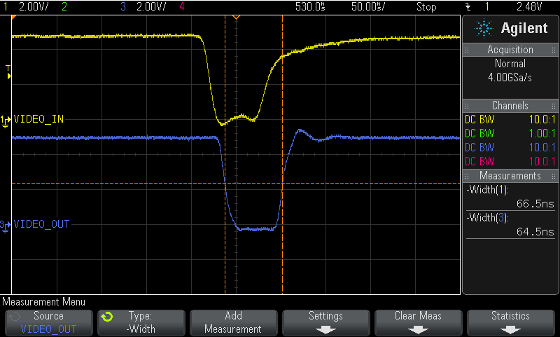 no perceptible difference on the screen. You’d expect to see a pulse width of 62.5 ns but I connected the probes with hooks and ground leads, which isn’t the right method for precise measurements at high frequencies (edit: and I had the bandwidth limited to 20 MHz). Good enough for this quick check, though. The output signal is about 20 ns late, which is caused by the propagation delay of the multiplexer and the NAND gates and is within the expected range (74HC257 typ. 10 ns @ 25°C; 74AC00 typ. 5 ns @ 25°C; 10 ns + 2 * 5 ns = 20 ns). (passed)
Step 5: Limit power supply to 100 mA; Insert the remaining chips; check current consumption and voltages.
Target: < 100 mA (all chips inserted)
Actual: roughly 65 mA (passed)
Target: 5.0 V
Actual: 4.97 V (passed)
Yippee! So far so good. Hardware has no severe faults. Now I’m going to setup the software development environment …