RC 2015/7 – Dances with Pixels #1

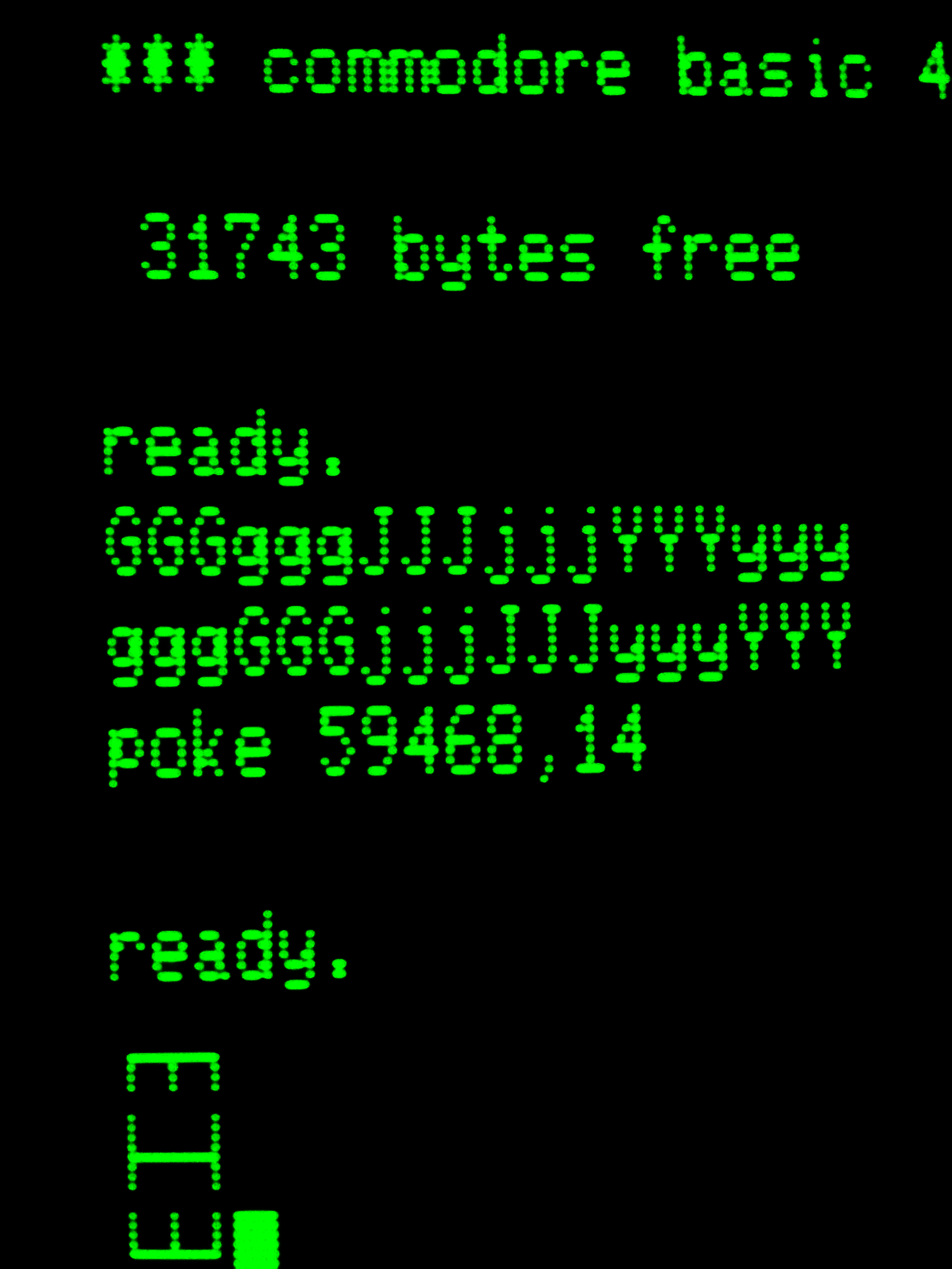
Engineer’s Log, Labdate 0725.22. Science Officer Spock finally managed to persuade the computer to accept the modification. We are traveling at warp 4.4 now. Warp 5 should be possible, though.

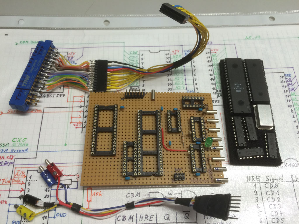
Ok, I swapped pins PE0 and PD0 to free an interrupt for VSYNC detection and added the interrupt service routine. Luckily vertical synchronisation worked right from the start. 🙂

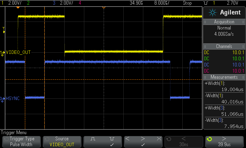
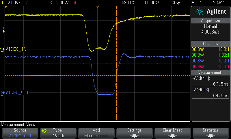
Sadly, tracking down the jitter problem isn’t that easy. At first glance it appeared to be a small difference in frequencies (main clock CBM vs. main clock HRE) so I tried to run the HRE on the CBM’s main clock and it improved somewhat. The jitter disappeared for one or two minutes to be precise – then returned. Cooling spray helped to locate the source of the problem: It’s the hex inverter chip (UD3) that forms the oscillator circuit. Really? I carefully examined the CBM text on the screen and there wasn’t any jitter at all. Only the HRE output showed jitter. Then I touched UD3 with my fingers and the jitter changed or disappeared. Unfortunately I have no spare finger to add to the circuit…

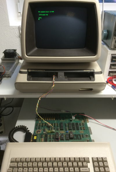
My provisional conclusion: The jitter is caused by the marvellous wiring and perfect grounding/shielding of the HRE board <ahem>.  As we are pinched for time I won’t design a proper PCB to solve this problem. Rearranging the cabling helps a bit…

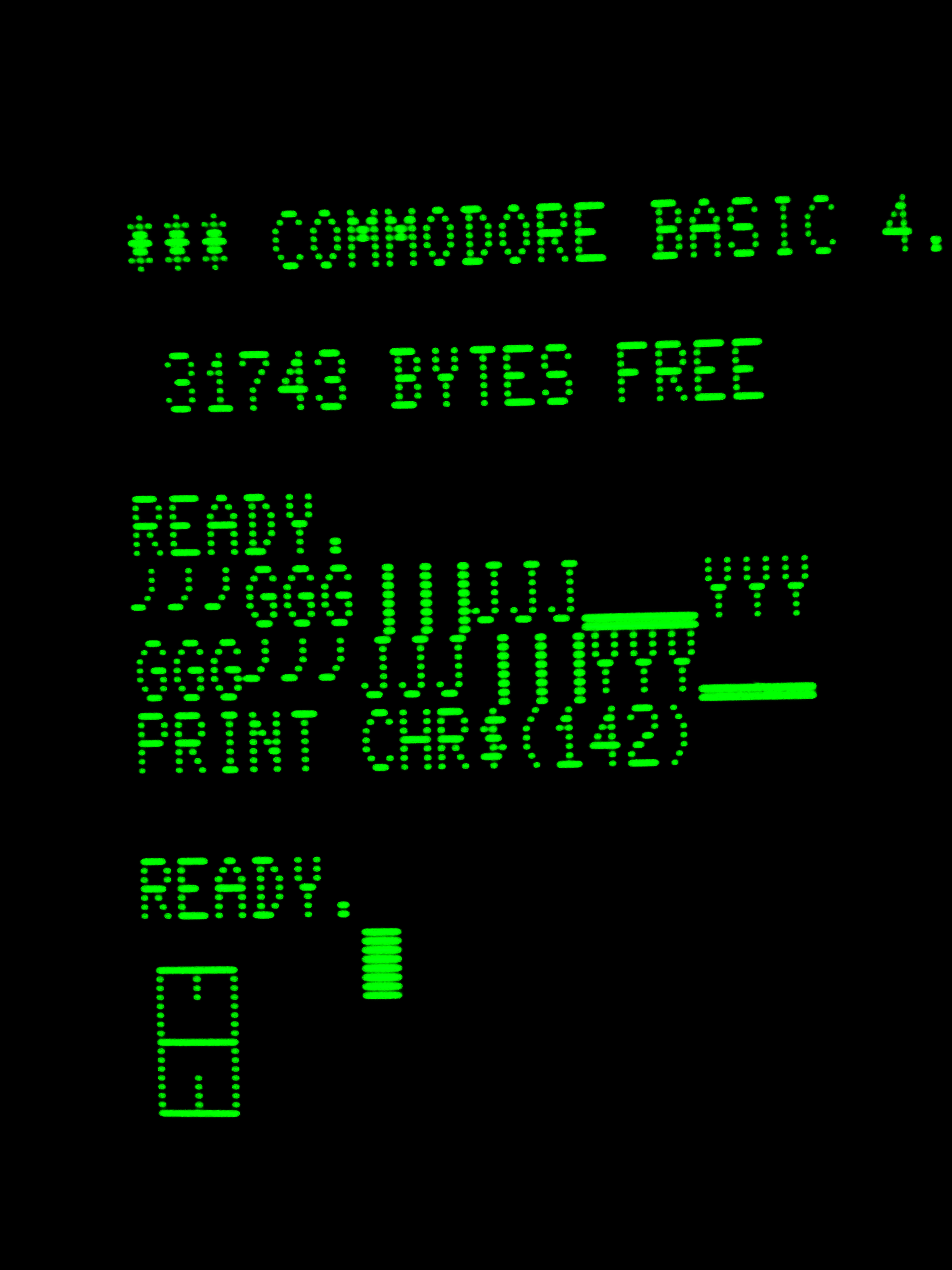
A screen full of equally spaced vertical lines is of avail when checking horizontal sync but otherwise quite boring. A screen full of freaking awesome vertical lines would require variable spacing! Easy! Just change the bit pattern and … fail.

For the first test I wrote a bit pattern to the external SRAM and imported the data in the next cycle to the shift register then clocked the bits out of the shift register to the monitor.

LDI  r25, 0b01111110  // load register 25 with bit pattern
ST    $8000, r25             //  store register 25 value into SRAM
OUT CtrlPort, r19         //  load data into shift register
OUT CtrlPort, r20        //  start clocking bits out of shift register
NOP                               //  waste one cycle

These six instructions take 8 cycles which is the time that is needed to clock 8 bits (pixel) out of the shift register. In other words 8 pixels are loaded and sent out to the monitor in 8 cycles thus allowing for a pixel frequency of 16 MHz.

Along with changing bit patterns for variable line spacing I coded a complete framebuffer handling as it will be needed for a graphic extension. Now I was reading the bit patterns from SRAM and then transferring them to the shift register. It turns out that the byte that has just been read from SRAM stays valid on the data bus for only one clock cycle (when /RD is LOW). The following OUT instruction cannot see this data anymore thus the transferred byte is not correct.

First idea was to send the data (that has been read into a microcontroller register) out to another port and import into shift register from that port. That would work if we had a free port.

Second idea was to handle the external SRAM manually but that would take much more clock cycles and reduce the horizontal resolution.

Third time is a charm: Enable XMEM, read bit pattern from external SRAM, disable XMEM, enable manual output on port A, send bit pattern to port A, import into shift register, start shifting. That results in 9 clock cycles which is still one cycle too many <Ҥ$+#%&/()!!!!> Fortunately the XMEM interface overrides any conflicting port definition if enabled and restores the old definition if disabled. So I could remove the port definition from the framebuffer read sequence and saved a cycle.

Meanwhile I wasn’t positive about vertical lines at all and programmed a bunch of sinewaves instead:hre02

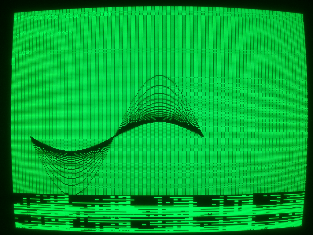
After some time of debugging the sinewaves appeared in a more pleasant fashion:hre03
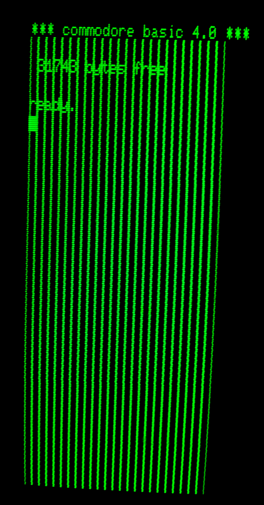
Men are like little kids so I played with my new toy:hre04
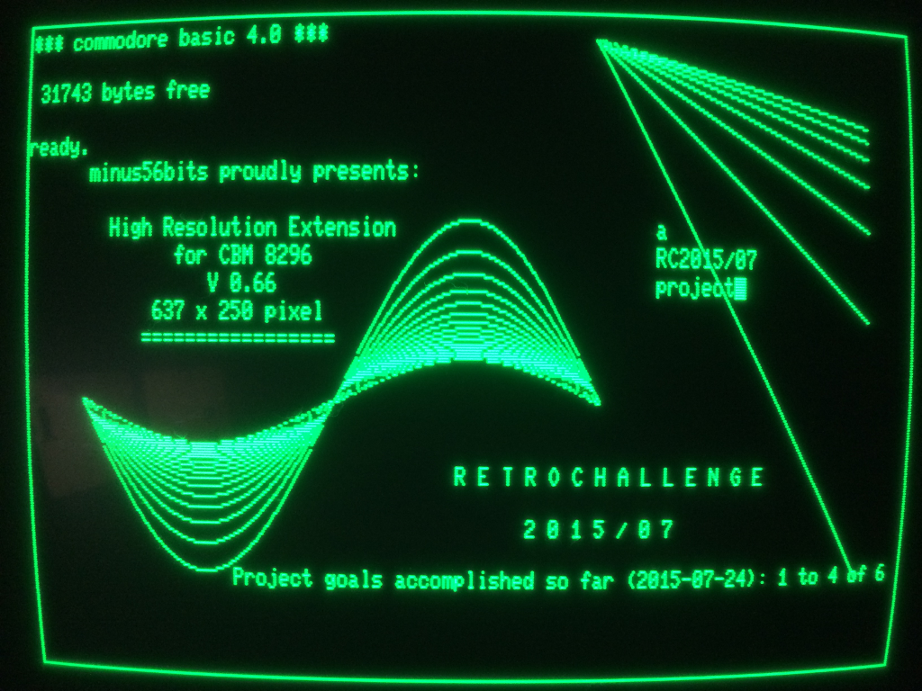
Border, lines and sinewaves have been computed by the HRE microcontroller. Text has been typed on the CBM keyboard. Due to the fact that the HRE has a separate video memory one can type and edit text/programs as usual without destroying the graphics. Current resolution is 637 x 250 pixels. Hopefully an additional debugging session will find the lost three pixels per line.

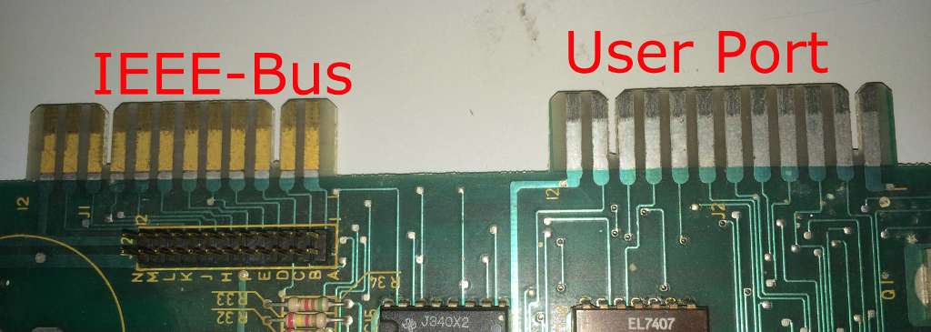
Implementation of the userport interface will be next. Stay tuned!

RC 2015/7 – Dances with Bits #2

Engineer’s Log, Labdate 0720.23. The Klingons wonder how we manage to stay combat-ready even if they prevent us from getting any sleep. I instructed McCoy to brew up some more of our secret weapon and to hand thermos out to the entire crew.

Yeah! After a slight hardware modification the HRE firmware can now display vertical lines that are aligned hre01with CBM characters.  Nothing to write home about but every little counts.

Vertical synchronisation will be next. Unfortunately I forgot to arrange for VSYNC detection. Oops! There is no pin with interrupt support left. Swapping PE0 / PD0 might help but that’s a task for tomorrow.

And I’ll hunt the jitter down … tomorrow.

Need some sleep badly…


RC 2015/7 – Dances with Bits #1

Engineer’s Log, Labdate 0719.21. Mr. Spock remarks that our computer underperforms even the human brain. That’s nice to hear.

I already had a look at LunaAVR about a year ago but haven’t used it for a real project until now. That’s simply because I haven’t worked on a private microcontroller project last year. LunaAVR has a nice IDE and comes with more than 300 pages of documentation as well as many example programs. There seems to be a small but informed and responsive community. After all it might be the right tool for the job.

Last night I tinkered a bit with the new release. It still lacks support for the external memory interface that I want to use. No big deal, though. Flipping some bits should turn XMEM on (it’s an Atmel term for eXternal MEMory)  and memory access will be handled by assembler anyway.

Where do we start? The CBM 8296 should behave as usual until a special command is issued to activate the HRE. For that purpose we have to set pin 9 of the shift register (output) to high level and pin 1 of the multiplexer (A/B switch) to low level so that only the CBM video signal is routed to the monitor. A 10k pulldown resistor takes care of the multiplexer but the shift register has no tri-state output and therefore the microcontroller must initialize the chip. While we’re at it: a subroutine for switching three video modes (CBM only / HRE only / both) would be nice.

Video synchronisation will be next.

IF you haven’t tinkered with video signals
THEN you might find the following (greatly simplified) abstract of avail
ELSE skip next four paragraphs

The CBM has a CRT (Cathode Ray Tube) monitor that sends an electron beam onto a fluorescent screen. The electron beam moves continually across the screen area in a fixed pattern starting at the upper left corner. It then moves horizontally to the right screen border, then back to the left border and down by the width of a pixel. This movement repeats until the beam reaches the bottom right corner of the screen. It then moves back to the upper left corner and the whole process starts again. In other words, the beam moves from left to right and line by line from top to bottom – just like you move your eyes while reading this text.

Three digital signals control the beam. In this text they are labeled VIDEO, HSYNC and VSYNC. One can’t see the beam as long as VIDEO is HIGH. If VIDEO is LOW then the fluorescent coating lights up at the current position of the beam. If HSYNC (Horizontal SYNChronisation) is HIGH the beam passes from left to right along the screen. If HSYNC is LOW the beam moves one line down and back to the left. HSYNC is like Carriage Return and Line Feed for the beam. While VSYNC (Vertical SYNChronisation) is HIGH the beam moves down the screen line by line. The beam returns to its home position (upper left corner) when VSYNC is LOW.

How do we display useful information? By precisely controlling the LOW periods of VIDEO. A long LOW period gives a long horizontal line and a short LOW period gives a short line. Our horizontal timing reference is the 16 MHz pixel clock of the CBM system. 16 Mhz pixel clock means that a single pixel has a duration of 1 / 16,000,000 s = 62.5 ns. Let’s assume we want to display a horizontal line of 8 pixels width. We then need to drive VIDEO LOW for 8 * 62.5 ns = 500 ns. A complete set of pixel information that can be displayed on the screen at a time is called a frame. The vertical timing reference is called frame rate (or refresh rate). It tells us how many frames per second will be displayed, that is how many VSYNC pulses occur per second. My CBM system uses a frame rate of 50 Hz.

Back in the days most computer monitors had quite simple (aka cheap) circuits inside. This tended to result in performance variations within a production lot and in temperature dependency of the display. Imagine they would have used the whole screen area to draw pixels and the start position of the beam moves slightly to the left while the monitor heats up. Some pixels would disapear behind the chassis of the screen. Thus borders were introduced to the timings.

hsync2v640This oscillogram shows a line of 640 bright pixels between two HSYNC pulses. The LOW period is 40 µs which is just what we expect (40 µs = 40,000 ns; 40,000 ns / 640 = 62.5 ns; 1/62.5 ns = 16 MHz). The HIGH period of 19 µs forms the horizontal borders. It takes about 16 µs from HSYNC going LOW to VIDEO_OUT going LOW and about 2.9 µs from VIDEO_OUT going HIGH to HSYNC going LOW. These periods define the horizontal position of the visible area.

To synchronize the HRE output with the CBM output I’ll use an interrupt that is triggered by HSYNC. Due to the fact that we have to be cycle exact in our timing we must take interrupt latency into account. The ATmega completes any ongoing instruction before an interrupt can be serviced. Since execution times vary from 1 to 4 cycles per instruction, an interrupt service routine has a random entry time. The solution to this problem is to put the µC into sleep mode. It then always executes the exact same steps when it wakes up and these will take always the exact same time to execute.


RC 2015/7 – Off Topic

Looking for debugging fun? How about this: Connect the RESET line of your microcontroller to an output pin that occasionally changes its level.

Yep. I’ve been there. Don’t ask me why. Maybe sunstroke while soldering. So much for “Hardware has no severe faults.”

RC 2015/7 – Enter Keyboard

Engineer’s Log, Labdate 0715.17. Warp engines are up and running again. Mr. Spock has a lively discussion with the computer on the options to unleash the engines’ full capability.

The soldering iron has cooled down bang on time. Half-time for the Retrochallenge. But there is no time for wild partying. Just one deep breath while downloading the recent version of LunaAVR which will be the programming language for this project. I like to try new languages and this tool sounds promising. One important feature is the inline assembler. When it comes to tight timing requirements I prefer assembler to any compiler optimization.

The LunaAVR IDE will work shoulder to shoulder with an AVR JTAGICE mkII in programming the ATmega162 microcontroller. This is my “hello world” program to test the build chain, the main clock and the microcontroller:

helloworld

… compiler output …

compile

… programmer output …

avrdude

… and the µC toggles the LED in 1 s intervals.

All systems nominal! 🙂

RC 2015/7 – Power Up

Engineer’s Log, Labdate 0715.14. We have stopped our engines for maintenance and upgrade. Mr. Scott is supervising the initial startup procedure of the new warp extension.

kitTadaaaah!!! Here it is: The Double Retro Kit! It’s double retro because it has been built entirely from parts out of my junkbox. 😉  I used my last card connector that fit the CBM/PET boards. In case you know a source where one can still buy these connectors, please drop me a line.

The 1:1 adapter from user port to pin header hasn’t been finished yet. The whole thing will have a bath in epoxy sometime.

WARNING! FOR ADULTS ONLY! AWFUL MESS OF WIRES AHEAD!

bmowYep! There are some very good reasons why not to build it like this. We have to handle high-speed digital signals (pixel stream, fast edges of 74AC00 and 74ALS573) and if this project were meant to be a consumer product, a proper PCB would be required. I consider this project to be a proof of concept and hope to get along with the direct wiring. I’m prepared to fix some weird issues that might pop up, though.

Ok, let’s populate the board step by step and do some checking. Maybe we can prevent it from catching fire. Please feel free to skip the rest of this post as it might be quite boring to read unless you are interested in the engineering part of the story (aka watching me putting my foot in my mouth).

Step 1: Limit power supply to 40 mA; check current consumption with empty sockets.
Target: < 1 mA
Actual: < 1 mA  (passed)

I’d like to see if the CBM video signal can pass the HRE board without interference. It enters the HRE at pin 2 of the multiplexer (74HC257) and is fed to the NAND (74AC00) afterwards. Let’s check that path.

Step 2: Insert 74HC257; check current consumption and voltages.
Target: < 1 mA
Actual: < 1 mA  (passed)
Target:  5.0 V
Actual:  5.0 V  (passed)

Step 3: Insert 74AC00; check current consumption and voltages.
Target: < 1 mA
Actual:  4 to 32 mA  (failed)
Target:  5.0 V
Actual:  5.0 V  (passed)

It seems as if we have some unwanted oscillation here. That’s ok because of currently floating inputs at pin 9 and pin 10. Does the current stabilize if we apply some pulldown resistors? Fortunately, yes. The current drops below 1 mA. (passed)

Step 4: Connect HRE to user port; start CBM; check video signal.
Target:  The signal should look quite the same after having passed the HRE.
Actual:  The output signal looks pretty good and there is vidinoutno perceptible difference on the screen. You’d expect to see a pulse width of 62.5 ns but I connected the probes with hooks and ground leads, which isn’t the right method for precise measurements at high frequencies (edit: and I had the bandwidth limited to 20 MHz). Good enough for this quick check, though. The output signal is about 20 ns late, which is caused by the propagation delay of the multiplexer and the NAND gates and is within the expected range (74HC257 typ. 10 ns @ 25°C; 74AC00 typ. 5 ns @ 25°C; 10 ns + 2 * 5 ns = 20 ns).  (passed)

Step 5: Limit power supply to 100 mA; Insert the remaining chips; check current consumption and voltages.
Target:  < 100 mA (all chips inserted)
Actual:  roughly 65 mA  (passed)
Target:  5.0 V
Actual:  4.97 V  (passed)

Yippee! So far so good. Hardware has no severe faults. Now I’m going to setup the software development environment …

RC 2015/7 – Aaarrgh!!!!

Engineer’s Log, Labdate 0713.10. I am at a loss for words. – Mr. Spock comments: “Fascinating is a word I use for the unexpected. In this case, I should think interesting would suffice.”

Isn’t this a nice connecting cable to the user port pin header?upcable1

Well, yes. It will definitely come in handy … IN CASE A USER PORT PIN HEADER HAPPENS TO GROW MAGICALLY ON TOP OF THE MAINBOARD SOME DAY!!!

ports1


RC 2015/7 – Fact-Finding #2

Engineer’s Log, Labdate 0712.21. Due to a severe galactic cosmic ray storm we were completely cut off from the Earth. Uhura picked up a weak radio signal from RC command today and we are confident that communication will be in normal state within hours.

I came up with some interesting ideas for the graphic extension project while digging into the details of the CBM video system, but: Too many ideas, too little time! So I’ll have to keep my hands off the more sophisticated topics for now and focus on a quite simple approach.

Ok, so what’s the final plan for this Retrochallenge?

  1. Name the thing to improve blog readability. I’ll call it High Resolution Extension and use the abbreviation HRE from now on. (done!)
  2. Construct a minimally invasive hardware. Avoid soldering at the CBM mainboard if possible. Use connectors instead.
  3. Consider it a success if a resolution of 320 x 250 can be accomplished but aim at a resolution of 640 x 250.
  4. Combine the CBM video signal and the HRE video signal so that the following modes can be used:
    – CBM text mode without any HiRes graphic (default)
    – HRE graphic mode without any CBM text
    – CBM text and HRE graphics combined
  5. Control HRE through the User Port (POKE).
  6. Integrate some kind of processing unit for simple drawing tasks (aka GPU) to unload the main processor.

Fortunately there is a connector between mainboard and monitor and all video signals are connected to the user port, so the HRE will get all input signals from the user port and output signals to the monitor connector. An external supply will deal with the power input.

It seems as if we start off on the right foot. Can we fulfill part two of our plan so easily? Maybe, but we’ll have to consider timing issues. The CBM pixel clock is 16 MHz. In other words, a single pixel is a 62.5 nanosecond flash. A side by side display of HRE and CBM pixels requires a very precise syncronisation of the two pixels streams. To be cycle exact we should use the exact same cycles. – Easy! Let’s connect to the mainboard’s clock pulse!

Beware! Besides the fact that there is no connector to the main clock (and soldering violates part two of the plan) it would be an open-heart surgery. The main clock controls every function of the computer and if our circuit introduces any kind of noise to the clock system, we might end up with an unreliable device. Therefore I dropped this option. I’ll go with a separate clock and synchronize to the horizontal sync pulse.

Hardware Overview

The GPU will be an 8-bit microcontroller clocked at 16 MHz. I want to keep some memory up my sleeve, so a 128k x 8 bit SRAM will join the microcontroller. Add a latch, a shift register, multiplexers and NAND gates and you’ll get the HRE. Hopefully.

schematic1Sorry. No complete schematic. And no PCB layout. Why not? Summer! We had beautiful weather here and I wanted to spend my spare time outdoors. Although I really enjoy PCB design, it’s a pain in the neck if you try it on a notebook in bright sunlight. Therefore a sketch on paper seemed appropriate and adequate. Doesn’t a real retro project need some retro design methods anyway?

The SRAM interface consists of

  • AD7:0  multiplexed low order address and data bus
  • A16:8  high order address bus
  • ALE  address latch enable
  • /RD  read strobe
  • /WR write strobe

A16 is used for bank switching given that the microcontroller (ATmega162) can’t address more than 64k of external RAM. The data bus is linked to a parallel in – serial out shift register (74HCT597) that converts the data byte into a serial stream of pixel bits. Shift register and microcontroller are clocked by a 16 MHz crystal oscillator. IC 74HC257 works as a digital switch. It connects either the CBM video stream or a pullup resistor to the NAND gates (74AC00) where CBM pixel bits and HRE pixel bits are combined to a single stream (see truth table). The user port is linked to a free port on the microcontroller.

The circuit will be soldered on a stripboard and has been almost finished. Stay tuned!

RC 2015/7 – Fact-Finding #1

Engineer’s Log, Labdate 0702.01. We have entered a spectacular binary star system in the Retrochallenge sector on a most critical mission of electronic research. Our mission is one of rescue and, if necessary, confrontation with a hostile force.

Scotty’s rule #setup11:
Never trust an ancient power supply.

Although the switching power supply seems to work ok, I wanted to add some reliability by using a benchtop power supply.

Removing the mainboard was easy but making an appropiate power adapter took me a while.

adapter1 My junk box offered no fitting connector, so I used three insulating screw joints (+12V, +5V, GND). Granted, it looks weird, but there is hardly any voltage drop across this connection.

However, there is a voltage drop of about 500 mV on the white wire. The small diameter of the original wires to the CRT (the blue and the red wire on the left) made me think there is only a small current flow, so I used the same diameter for the +12V line to the power supply. Shame on me. Every child knows

Scotty’s rule #2:  Never underestimate the wattage of a CRT.

Anyway, the computer is up and running and we can start to investigate details of the CBM video system.

The model 8296 can display 25 rows of 80 characters in two modes, a text mode and a graphic mode. Don’t get confused by the term “graphic mode”. In CBM language it refers to several special characters that can be used to draw very limited line or block graphics (see example at the bottom of the following two pictures) and does not mean that you can plot arbitrary waveforms in pixel resolution (aka HiRes graphics). The latter is what this project is about.

Ok, let’s calculate the screen resolution in pixels. A single character is composed of 8 x 8 pixels, so the horizontal resolution is 80*8=640 pixels. The vertical pixel resolution depends on the current mode:

In text mode there are additional vertical gaps of twotextmode1pixels between the rows to improve readability.

These gaps disappear  in graphic mode.graphmode1Therefore we get a vertical resolution of 25*(8+2)=250 pixels in text mode and a resolution of 25*8=200 pixels in graphic mode. Screen resolution is then 640*250=160,000 pixels at most (non interlaced) and it would take 160,000/8=20,000 bytes to buffer one HiRes page. Double that for interlaced mode.


RC 2015/7 – Setting Objectives

Marketing Department claims that we are in need of a marvelous project name and an infinite list of dazzling features. Financial Department moans that throwing money onto a dead technology won’t result in a rebirth. General Management commands overtime to meet the deadline July 15th.
<plop>
Development Engineer thinks it’s great to awake from a nightmare.

Ok, so why, what and how?

Why? Well, I own a small collection of PET/CBM series models and want to learn as much as possible about their working principles to keep these beauties running. Detailed knowledge is essential as more and more spare parts become Unobtainium. The development of a graphic extension and its integration into
the CBM video system will most likely teach me something.

What? That’s still a moving target. I simply don’t know how the video system works and what can be accomplished within a few weeks. Possible goals are
– resolution better than 240 x 240 pixel
– different pixel states (e.g. off, dim, normal, bright, blinking)
– integrated character generator
– scalable character size
– integrated graphic processor
– 4D accelerator, VSXGI, MXFAA, DSQR, 8K, VR INDIRECT (that’s for the marketing guys)
– simple interface to CBM BASIC

How? Study the circuit diagrams. Use the oscilloscope. Surf the internet. Refine the goals. Sketch a circuit. Avoid SMD parts. Start soldering already!

REPEAT
fix the errors
don’t give up
UNTIL success OR deadline