RC 2017/10 – 6522 inspection

In addition to the IEEE-488 bus the Commodore PET/CBM series features an 8-bit parallel interface named Userport. A single 6522 Versatile Interface Adapter (VIA) provides bidirectional I/O lines, two 16-bit timers and an 8-bit shift register for serial communications.

The monochrome High Resolution Extension (RC 2015/07) used a parallel protocol for Userport communication. In theory we could use it with CHRE as well since there are eight free I/O pins left on the ATmega (four pins of the programming header included). But I hope to keep a few extra clock cycles on the ATmega if I use its USART (Universal Synchronous/Asynchronous Receiver/Transceiver) hardware support for serial communication.

Only a few cycles? So why bother about it at all? Well, lets compare the requirements:

HRE:
resolution 640 by 250 pixel
one BIT per pixel (monochrome)
20,000 bytes per frame
50 frames per second
data transfer rate about   1 MByte per second

CHRE:
resolution 640 by 480 pixel
one BYTE per pixel (256 colors)
307,200 bytes per frame
60 frames per second
data transfer rate about 18 MByte per second

The CHRE microcontroller is somewhat more stressed due to this tiny difference. It has to spend a lot more processing power on the job. This leaves us with only a small amount of time to

  • do PET communication,
  • decode, verify and dispatch the received drawing commands,
  • do the rendering.

For example, it took nearly ten minutes (!) to render the screen content that I posted the other day. Granted, there is room for firmware improvement, but it definitely makes sense to be picky about the use of clock cycles.

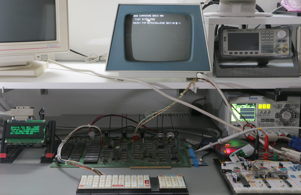
It is said that the 6522 VIA shift register will lose a bit if an externally supplied shift clock edge falls within a few nanoseconds of the falling edge of the internal clock. So maybe the shift register won’t bug me if the internal I/O clock is used?  I’m sure there is a comprehensive discussion about this issue somewhere on the internet, but I couldn’t find it. Oookay, you’ve got me! I’ve done no more than a superficial search, because I’d like to play with the scope. The official statement is: I need to know if the VIA in my PET is functional at all. 😉

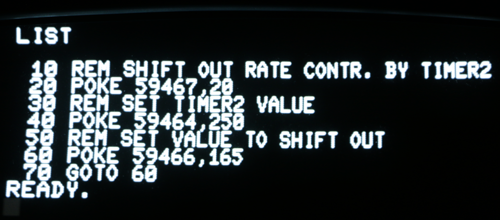
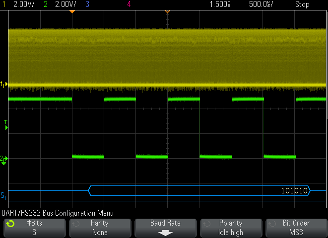
We don’t have to comply with any standard here, so we start the test with a bit rate of 2,000 bit/s. The VIA setup is done by a short BASIC program:

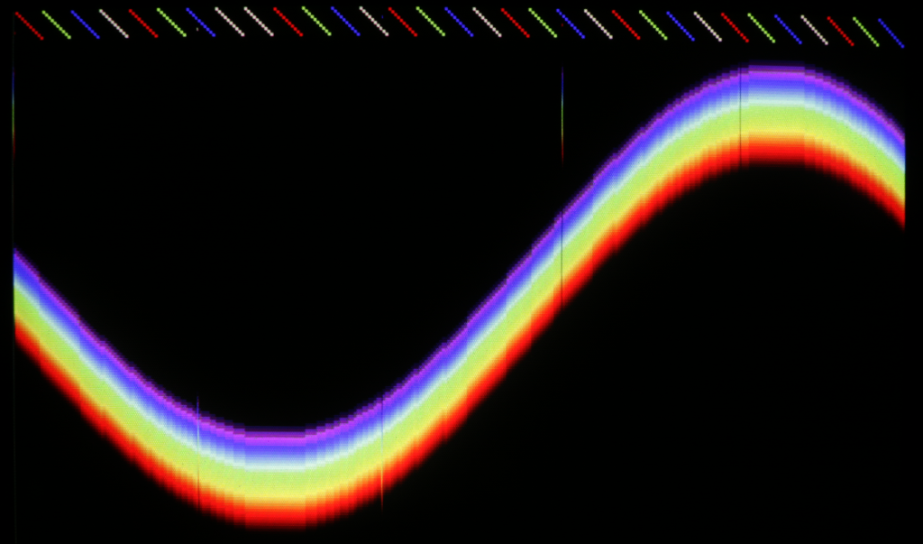
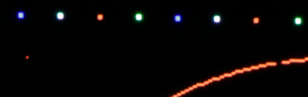
Let’s look at the clock signal first:

Ch1:  internal I/O clock (phase 2)
Ch2:  output shift register (bitstream)
S1:  decoded bitstream (binary)

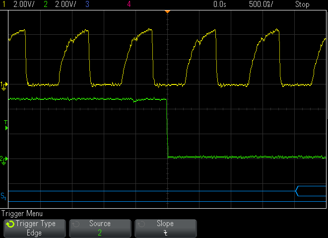
Ohuuu, that’s not exactly the most rectangular square wave I’ve ever seen, I’m afraid. However, surprisingly the VIA doesn’t seem to care! The bit stream looks quite good at first glance:

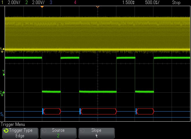
Yep, there’s a problem with the second glance: Now you wish you had stuck to the first one. Anyway, we have to note the absence of any decoded data. The empty red boxes are a polite indication that

a) the VIA is really faulty,
b) the creature in front of the scope made a suboptimal decision.

Make an educated guess…

… It’s  b).  Using 8 bit data wasn’t clever.

The shift register in this VIA is just an 8 bit shift register, no complete UART/USART. It does not send a leading start bit and does not send a trailing stop bit either. Without a start bit the scope cannot detect the beginning of a frame and therefore cannot decode the bitstream.

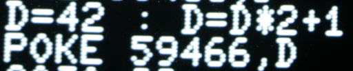
A slight modification to the BASIC program reduces the usable data length to six bits. The answer to all questions is stored in variable D (binary 00101010). We multiply by 2 (result: binary 01010100) and add 1 (result: binary 01010101). The MSB is now zero (aka start bit) and the LSB is one (aka stop bit).

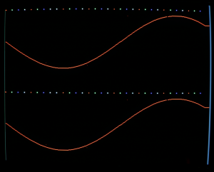
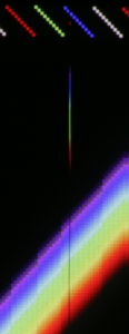
Now the scope decodes the data:

To find out if there is some kind of rare glitch we use the mask test function of the scope:

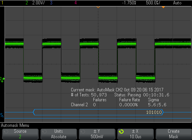
I’ll call that a promising result. When cranking up the bit rate to 250 kbit/s we get the same good result. So we may assume that at least an unidirectional serial communication is possible…


RC 2017/10 – Schematic

Now that the graphics circuit seems to work, I should give you an overview of the current state of the hardware. Please match this picture of the breadboard

with this

preliminary schematic

The position of the components on the breadboard is roughly reflected in the circuit diagram.

VGA synchronising is handled by PB0 (horizontal sync, pink wire) and PB1 (vertical sync, brown wire).

Latch U2 separates the pixel data bus (Color0..7) from the digital to analog converter during the blanking periods when the microcontroller sends pixel data from Port A to the SRAM. U2 is controlled by PD6. SRAM read/write mode is controlled by PD4.

The address bus is partly multiplexed. PB2 selects the most significant address bit (Addr18). PB3 switches latch U3 into transparent mode, then Port C puts address bits 10 to 17 on the bus, then PB3 switches U3 into latched mode, then Port C puts address bits 2 to 9 on the bus and PD7 / PD5 deliver Addr0 / Addr1.

While streaming pixels from SRAM to the screen Port A is in high impedance state and U2 in transparent mode. Three simple R2R resistor ladders convert the digital color information into analog voltages. Eight shades of red, eight shades of green and four shades of blue make 256 colors in total.

I haven’t decided how to connect to the PET yet. I would like to utilize a shift register in the 6522 interface chip as I have two serial ports available on the ATmega, but unfortunately the 6522 has at least one major bug. From what I’ve read so far it seems that the error only occurs when an external clock is used. Exhaustive tests have to be performed, I’m afraid. Time to play with the EEs best friend… 😉


RC 2017/10 – MARVEL !!!

Please excuse the lurid headline. I’m overwhelmed with emotion! I was already soooo close to the ultimate goal at the end of spring-time RetroChallenge – but couldn’t see it!

This evening, while exploring sourcecode and breadboard circuit for the first time after several month, the scales fell from my eyes!

After some minor changes this really simple circuit now displays 640 by 480 pixels at 256 colors on the VGA screen!!!

Well, it’s slow as a footsore snail on sleeping pills, but that doesn’t diminish my rapture.  🙂


RC 2017/10 – Getting started

Ok, I finally found some time to get the project started. Better late than never! Not much to report, though. Just the usual tasks before real work can take place:

  • create space on the workbench
  • rake PET and breadboard up
  • find documentation (if available at all)
  • connect everything
  • download/install/configure toolchain
  • cupato (cheer up, pray and turn on)
  • REPEAT pull_a_long_face UNTIL all_bugs_fixed == true

I was pressed for time (aka lazy) last RetroChallenge, so I failed to realize that it would have been a fantastic idea to clean not only the 6520 socket but every chip and socket on the contaminated PET mainboard. The PET refused to start the BASIC interpreter and soft-landed in TIM. Tough luck! Fortunately a retro computing nerd agreed to do the cleaning – grumpily…

The PET seems to be ok now but the breadboard lives up to it’s name – not a single pixel is displayed on the VGA monitor. Monitor is ok when connected to a PC. Maybe the firmware version does not fit the last modifications of the circuit? To be honest, I probably missed to document the last steps as I hoped to continue the project on the next day. Apparently, it took about five month – and memory fades away…

In case you’re new to this project (or your memory is teasing you as mine does in this case), please consider (re)reading the archived blog entries of RC 2017/04 where I discussed some project basics. Otherwise it might be difficult to follow this ongoing development. Anyway, please feel free to put your questions into the comments. Moderated comments are used to prevent spamming, so it’ll take some time before your comment gets published.

RC 2017/10 – PET/CBM Color Graphic again

At the beginning of RC 2017/04 I promised my dearly beloved PET 2001 that it will be transformed into a Color-PET this year. I stand by my promise.

Spring-RetroChallenge lead to a color graphic system on a breadboard. It was capable of displaying 320 by 240 pixels at 256 colors on a VGA monitor. Besides a few quirks it worked quite reliable but was not connected to the PET at all.

During this RetroChallenge I plan to get rid of the remaining bugs, integrate the graphic system into the PET and write a BASIC extension that supports graphic primitives like DrawPixel, DrawLine, ClearScreen, etc.

RC 2017/04 – After-Show Party

What caused the toasted port on the microcontroller? I’m working always on a electrostatic dissipative mat, so the only possible reason is a conflicting situation on the data bus. I found a sequence in my source code where Port C of the controller and the external SRAM were both set to output. Shit happens!

I modified the circuit so that the output enable pins of the SRAM and the DAC-latch are connected, hence now the SRAM is driving the data bus only during the active periods of a frame. That limits my chances of spoiling the circuit again as there is simply no time to fool around when every cycle counts.

Today I replaced the defective ATmega1284 by a new one, adjusted some fuses, burned the last development version of the firmware aaaand look what we’ve got:

Yeah! Now we are talking!  🙂

It’s far from being perfect, but it’s doing much better than I expected. Only a few unplanned pixels due to EMI are visible (see below: the small red dot on the left).

There is a discontinuity in the sine wave at x = 256 and if you look closely you’ll notice a slightly greater distance between the red pixel and the green pixel above that gap than between the other pixels. This might be an off-by-one error in the pixel drawing routine or the result of two more clock cycles when switching to the next memory page (256 bytes). The sine wave ends in a flat line, which most likely means the shut-off of the DAC is late. I have currently no clue where the blue-grey vertical lines in the leftmost / rightmost positions come from, though.

I must admit that the desperate hurry during the last few days of RetroChallenge left me with a suboptimal wiring scheme.  My decision to use a single port for the low byte and high byte (via a latch) of the address wasn’t particularly favorable. Every pixel has to be drawn within two clock cycles. That works fine until the address counter of a line reaches 255. Now we need to increment the high byte of the address and set the low byte to zero:

– increment address high byte register (1 cycle)
– set transparent mode (1 cycle)
– output address high byte register (1 cycle)
– set latched mode (1 cycle)
– clear address low byte register (1 cycle)
– output address low byte register (1 cycle)

Obviously that does not fit. Here is my workaround:

– set address pin A16 to high (2 cycles)

It works, but the resulting memory scheme is weird:

0, 1, 2, 3, … 255, 65791, 65536, 65537, 65538, … 65598

Ok, it’s not as bad as it looks like at first glance. Every memory scheme is just a human conception/idea. The memory chip doesn’t care about the address sequence at all. As long as we use the same address when reading or writing a specific byte everything is honky-dory. However, we waste 192 bytes per line this way. Version 2.0 of CHRE will take care of this issue…

In fact, the gap we’ve seen in the sine wave was caused by an off-by-one bug and wasted cycles. And the DAC-latch timing was wrong. Both issues could be fixed easily. In addition the vertical resolution has been reduced from 480 to 240.

So, now we have 320 by 240 at 256 colors! That was one of my goals for RetroChallenge. Accomplished. But way too late. 🙁

Anyway, playing with this graphics board is fun:

Unfortunately we see some spooky vertical lines now…

                    To be continued…

RC 2017/04 – Inspection Report

Despite good progress made by shoving bits in my software development tool of choice, finally the CHRE firmware resisted the plan to show at least some real color graphics before the end of RetroChallenge. So, I waved the white flag, took some sleep and got back to the issues today.

When sending video data from the MCU straight to the DAC it was possible to produce some nice looking pictures:

A closer look to the color gradient…

Ok, that’s boring, but nice. This graphic shows a resolution of 320 by 480 at 16 out of 256 colors. Apparently, we have a rock-solid timing. Edges are well defined and no distortions are visible.

Unfortunately as soon as I try the same out of the video memory nothing works as expected anymore. To make a long story short, it turned out that I somehow managed to fry Port C of the ATmega1284. Its output drivers are still working, but it draws about 6 mA on each pin in high impedance state. That pulls every bit of data down that the SRAM tries to send to the DAC.

I will continue to work on this project as time permits. Please follow me on Twitter or check back regularly.

By the way, if you are interested in some other PET 2001 work regarding graphics, make sure to visit the awesome RetroChallenge 2017/04 project of Norbert Landsteiner, who implemented a “Space Commander” clone based on character graphics! Hats off to Norbert!

RC 2017/04 – Alternative Schematics

Time is short so let’s skip the part where we draw schematics. I thought it would be more fun to show you how the circuit develops and explain it along the way.

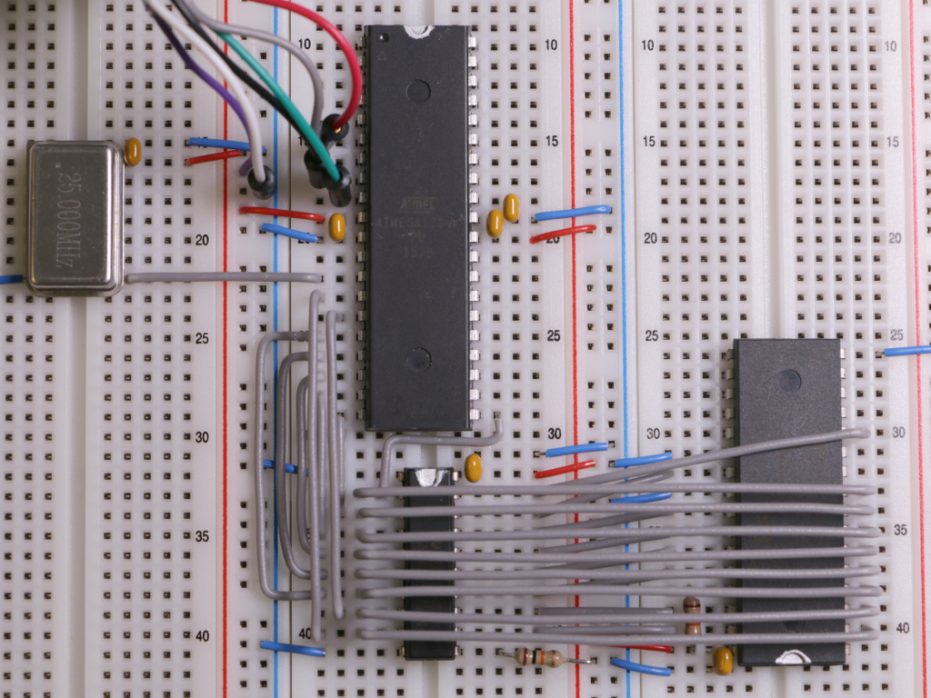
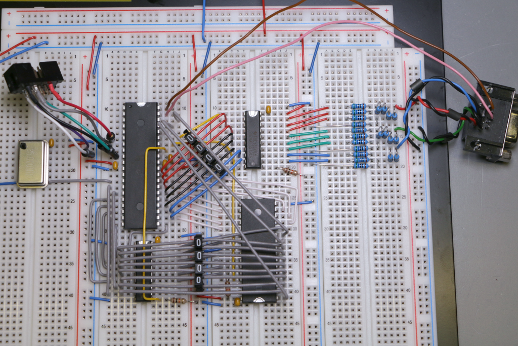
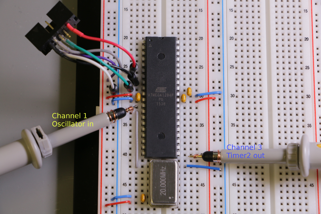
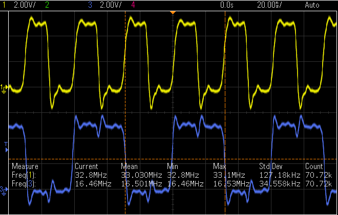
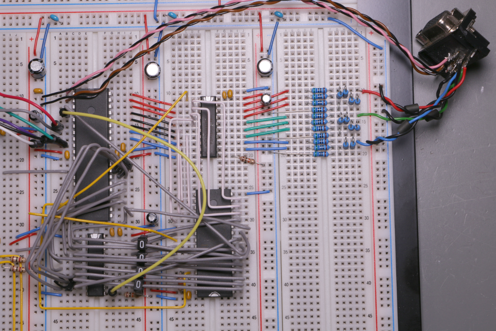
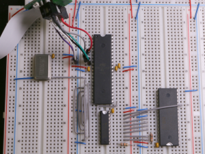
A golden rule in (high speed) digital circuit layout is to keep wires/traces as short as possible and to increase the spacing between adjacent wires/traces. That helps to reduce electromagnetic interference, e.g. cross talk. Therefore the previously used test circuit has been rearranged to get the oscillator out of the way. The grey wire between the silvery can on the left and the biggest chip on the board is our clock line feeding a square wave of 25 Mhz @ 5 Vpp into the ATmega1284.

Blue wires are  signal ground,
red wires are  supply voltage,
grey wires are  address lines and clock lines,
white wires are data lines ,
yellow wires are control lines,
(SCNR, read: ‘data lines’ and ‘control lines’)
beige drops are  decoupling caps,
beige or blue cylinders with colored stripes are  pull-up resistors,
unless otherwise noted.

First exception: A bunch of colorful wires is leading to a connector and a flat flex cable at the top left. These are used to program the microcontroller (MCU).

There’s an address latch (74ALS573) below the MCU. Yes, I know. The ALS type is too fast for the task and may cause additional EMI issues. Unfortunately I don’t have (or can’t find) the HC type. Living countryside doesn’t help when trying to buy electronic parts on a weekend either.

The external SRAM (BS62LV4006) is situated on the right. Nineteen address lines are required to access the full 512KB. Add eight data lines, eight lines for communication to the user port of  the PET 2001, three control lines, two video sync lines and you’ll get  ERROR! OUT OF I/O PINS!  The solution is a buffer store aka latch:

Port D of the ATmega is connected to the SRAM via the address latch. Thus it can output the first byte of an 19-bit-address while in transparent mode, then switch to latch mode. The address latch keeps this bit pattern on its output pins, regardless of any state changes on its inputs until it is switched back to transparent mode. Now Port D can output the second address byte.

Additional eight wires are routed from Port D to address pins on the other side of the SRAM.

Avoiding long wires means implementing a second layer. This is a small, easy project on a breadboard.

Now we connect Port C to the data bus…

… and add a simple R-2R resistor ladder network as Digital Analog Converter (DAC):


Please note that there is a second latch! It will separate the data bus from the DAC while data is written to the SRAM, because otherwise we would get flicker at least. Most likely the horizontal and/or vertical synchronisation would fail.

The last picture shows the complete CHRE circuit including a third layer of address lines, five control lines (latches, SRAM Read/Write, Hsync, Vsync) connected to Port A and some spacers on the second layer.

Now on to firmware development. Hurry up!!! Only 1.5 days to go…

RC 2017/04 – Breadboard Time

It’s a matter of common knowledge that a breadboard isn’t suitable for high frequency circuits. But 0.025175 GHz is almost DC, right? Not at all! In particular, one will find fast edges, even in most digital circuits that are clocked really slow. It’s not only the system clock we have to worry about when prototyping on a breadboard. These fast edges may contain high frequency components up to several hundred MHz.

Nevertheless I’ll start on a breadboard. Why? To test a few things before going any further. Okay, maybe there is also a tiny bit of curiosity involved. 😉

But before we go to the breadboard we need to do some math. Please stay with me! It’s basic arithmetics only. Promise!

The PET displays 40 x 25 characters using an 8 x 8 pixel monospaced font. The corresponding screen resolution is
40 * 8 = 320 pixels horizontal,
25 * 8 = 200 pixels vertical.
Having this resolution for color graphics would be great, as we could print text in the original PET font side by side to color graphis at the exact same pixel size.

As mentioned before a horizontal resolution of 640 pixels equals to a Dot Clock of about 25 MHz in the VGA universe. For a resolution of 320 pixels the Dot Clock is halved, too (25 Mhz / 2 = 12.5 MHz). The plan is to store the color of a pixel in a single byte, so 2 * 2 * 2 * 2 * 2 * 2 * 2 * 2 = 256 colors are possible (Sorry, but I had to keep a promise. For really advanced mathematicians out there that is 2^8).  Thus the circuit will have to spit out a byte per pixel – that is 12.5 megabytes per second!

All video data resides in external RAM. Transfering a byte (pixel) from external RAM to the DAC (Digital Analog Converter that converts pixel data into VGA compatible voltages) requires four steps:

Precondition: RAM is in read mode

1) calculate RAM address
2) feed address to RAM
3) read color byte from RAM
4) send color byte to DAC

Assuming that each of these steps takes a single clock cycle, a system clock of 4 * 12.5 MHz = 50 MHz is needed. The ATmega1284 is rated for a maximum clock frequency of 20 MHz. Oops.

Fortunately two of these steps are unnecessary. We can avoid steps 3 and 4 by connecting the external RAM data bus straight to the DAC. The microcontroller will act merely as a counter then. Wouldn’t it be easier and cheaper to perform this task with a standard resettable counter chip? Well, it’s possible for sure (PET 2001 video circuit consists of 74xxx logic only), but in my view it’s more convenient and flexible to substitute a microcontroller for a bunch of logic chips here. Anyway, in both cases we end up with dealing with two logical steps. The question is if the above assumption is true: How many clock cycles does the ATmega really take to perform these steps? Ooookay, the party is over! We’re talking assembler and count cycles from now on…

Come on! Stop crying! Real programmers do talk assembler and do count clock cycles. End of story.

The ATmega1284 datasheet (in fact it’s more of a databook), chapter 29, Instruction Set Summary, is our friend: It takes one cycle to increment or decrement a register and it takes one cycle to output a register value to an I/O port. Therefore a pixel can be addressed in two clock cycles. That’s great news! Assumption verified! We need a system clock of only 2 * 12.5 MHz = 25 MHz. …
Only? That’s still 5 MHz more than the 20 MHz the ATmega is specified for.

Guess what? First task on the breadboard will be pushing the ATmega1284 to its speed limits. I’ve done overclocking on other AVR chips before. A stable external oscillator is key to maximum speed. The test circuit is pretty simple:

Just the controller, an external crystal oscillator, a bunch of capacitors, a programming header and two oscilloscope probes. All tests will be done at 5 volts. We start at 20 MHz to make sure everything is working correctly when the clock is within specification.

The program is quite simple as well. It’s the setup of Timer2 to toggle PD7 on compare match and an endless loop doing nothing:

According to the datasheet this configuration is specified for a maximum toggle frequency of SysClk / 2. A quick look at the scope verifies that the frequency at PD7 is about 10 MHz. So far so good.

Now we’ll raise the frequency until the circuit stops working correctly. My junk box offers 25, 28.322, 32, 33, 36, 40, 48 and 50 MHz…

Tataaa!!! Aaand the winner is:

33 MHz!!!

Wow! That will give us a reasonable safety margin when running at 25 MHz!

Only three days left and counting…

RC 2017/04 – Real Deal

Although I enjoyed to see the PET 2001 being safe and sound again, it was no big deal as most of the work had been done before this RC. The real challenge will be to build a color high resolution graphics extension board for the Commodore PET 2001 and some later models of the PET/CBM series. I’ll name that board ‘CHRE’ for ‘Color High Resolution Extension’ to illustrate it’s affinity to my RC 2015/7 project (HRE) which was monochrome only.

In contrast to the Commodore C64 the PET/CBM 2000, 3000, 4000 and 8000 models were not equipped with pixel graphics or color at all. Therefore we cannot enhance any internal system, we’ll have to start from scratch. What kind of screen should we use? TV-set? 4k curved OLED? The latter isn’t really a retro thingy, so no. A telly would fit to the 40 characters per line of a PET 2000, 3000 and 4000 model but I’d like to support an 80 column text mode (monochrome) for the 8000 models some day. While it’s possible to display 80 columns on a TV-set, the readability won’t be great. Thus we’ll cancel the telly and stick with a more modern standard called VGA. VGA monitors are still available at stores and The Bay. You may find a VGA input connector even on some present-day display systems.

VGA supports multiple resolutions and color modes. There are two limiting factors when it comes to graphic modes:
1) Dot Clock (frequency with which pixels are illuminated on the screen)
2) Video RAM (memory where pixel data is stored).

For a very common VGA mode of 640 by 480 pixels by 256 colors we would have to deal with a Dot Clock of 25.175 MHz and would need 307200 bytes of Video RAM (for you youngsters out there: that is 0.025175 GHz and 0.0003072 GB). Our PET/CBM CPU is an 8 bit processor running at about 1 MHz. Its max. address space is 64 KB. Even 160 by 120 pixels would require a Dot Clock of more than 1 MHz. Magic aside, how can we support any useful VGA mode? Well, we’ll need some kind of GPU and external RAM.

I’ve choosen the Atmel megaAVR series of 8 bit microcontrollers for the GPU. The biggest (in terms of I/O pins and features) and fastest (in terms of instructions per second) controller of this series is the ATmega1284. That’s not exactly true as its little brother ATmega644 needs a cycle less at jump instructions. It remains to be seen if these few cycles are relevant when calculating any time-critical parts of the firmware (aka cycle counting). The external VRAM will be a BSI BS62LV4006PCP55. That’s a 512K x 8 bit 55ns CMOS SRAM in a PDIP-32 package. The first homecomputers with color graphics used weird memory layouts to cope with memory and speed constraints. Our blisteringly fast GPU and nearly infinite VRAM will hopefully allow for a nice memory layout…

So the plan is to head for the following goals:

– color graphics mode with 160 x 200 pixel resolution at 16 colors or better
– color text mode with 40 x 25 characters at 16 colors or better
– minimally invasive connection to the PET 2001
– implement simple graphic functions in GPU firmware
– implement PET control software as a BASIC extension

Only 8 days left. Oops!